MSP430F530x, MSP430F5310
SLAS677B –SEPTEMBER 2010–REVISED MARCH 2011
www.ti.com
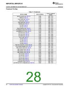
Peripheral File Map
Table 17. Peripherals
OFFSET ADDRESS
RANGE
MODULE NAME
BASE ADDRESS
Special Functions (see Table 18)
PMM (see Table 19)
0100h
0120h
0140h
0150h
0158h
015Ch
0160h
0180h
01B0h
01C0h
01E0h
0200h
0220h
0240h
0320h
0340h
0380h
03C0h
0400h
04A0h
04C0h
0500h
0510h
0520h
0530h
05C0h
05E0h
0600h
0620h
0740h
08C0h
0900h
000h - 01Fh
000h - 01Fh
000h - 00Fh
000h - 007h
000h - 001h
000h - 001h
000h - 01Fh
000h - 01Fh
000h - 001h
000h - 002h
000h - 007h
000h - 01Fh
000h - 00Bh
000h - 00Bh
000h - 01Fh
000h - 02Eh
000h - 02Eh
000h - 02Eh
000h - 02Eh
000h - 01Bh
000h - 02Fh
000h - 00Fh
000h - 00Ah
000h - 00Ah
000h - 00Ah
000h - 01Fh
000h - 01Fh
000h - 01Fh
000h - 01Fh
000h - 01Fh
000h - 00Fh
000h - 014h
Flash Control (see Table 20)
CRC16 (see Table 21)
RAM Control (see Table 22)
Watchdog (see Table 23)
UCS (see Table 24)
SYS (see Table 25)
Shared Reference (see Table 26)
Port Mapping Control (see Table 27)
Port Mapping Port P4 (see Table 27)
Port P1/P2 (see Table 28)
Port P3/P4 (see Table 29)
Port P5/P6 (see Table 30)
Port PJ (see Table 31)
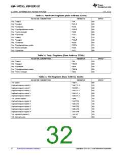
TA0 (see Table 32)
TA1 (see Table 33)
TB0 (see Table 34)
TA2 (see Table 35)
Real-Time Clock (RTC_A) (see Table 36)
32-bit Hardware Multiplier (see Table 37)
DMA General Control (see Table 38)
DMA Channel 0 (see Table 38)
DMA Channel 1 (see Table 38)
DMA Channel 2 (see Table 38)
USCI_A0 (see Table 39)
USCI_B0 (see Table 40)
USCI_A1 (see Table 41)
USCI_B1 (see Table 42)
ADC10_A (see Table 43)
Comparator_B (see Table 44)
LDO-PWR and Port U configuration (see Table 45)
28
Submit Documentation Feedback
Copyright © 2010–2011, Texas Instruments Incorporated

 TI [ TEXAS INSTRUMENTS ]