MSP430F530x, MSP430F5310
www.ti.com
SLAS677B –SEPTEMBER 2010–REVISED MARCH 2011
Universal Serial Communication Interface (USCI)
The USCI modules are used for serial data communication. The USCI module supports synchronous
communication protocols such as SPI (3 or 4 pin) and I2C, and asynchronous communication protocols such as
UART, enhanced UART with automatic baudrate detection, and IrDA. Each USCI module contains two portions,
A and B.
The USCI_An module provides support for SPI (3 pin or 4 pin), UART, enhanced UART, or IrDA.
The USCI_Bn module provides support for SPI (3 pin or 4 pin) or I2C.
The MSP430F53xx series includes one or two complete USCI modules.
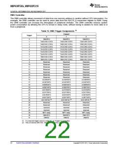
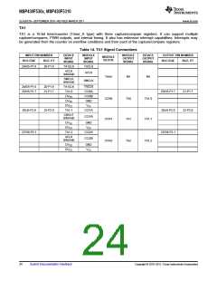
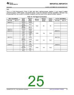
TA0
TA0 is a 16-bit timer/counter (Timer_A type) with five capture/compare registers. It can support multiple
capture/compares, PWM outputs, and interval timing. It also has extensive interrupt capabilities. Interrupts may
be generated from the counter on overflow conditions and from each of the capture/compare registers.
Table 13. TA0 Signal Connections
INPUT PIN NUMBER
DEVICE
INPUT
SIGNAL
MODULE
INPUT
SIGNAL
MODULE
OUTPUT
SIGNAL
DEVICE
OUTPUT
SIGNAL
OUTPUT PIN NUMBER
RGC/ZQE RGZ, PT
MODULE
BLOCK
RGC/ZQE
RGZ, PT
18/H2-P1.0
14-P1.0
TA0CLK
TACLK
ACLK
(internal)
ACLK
Timer
CCR0
NA
NA
SMCLK
(internal)
SMCLK
18/H2-P1.0
19/H3-P1.1
14-P1.0
15-P1.1
TA0CLK
TA0.0
DVSS
TACLK
CCI0A
CCI0B
GND
19/H3-P1.1
20/J3-P1.2
15-P1.1
16-P1.2
TA0
TA0.0
DVSS
DVCC
VCC
20/J3-P1.2
16-P1.2
17-P1.3
TA0.1
CCI1A
ADC10 (internal) ADC10 (internal)
(1)
(1)
CBOUT
(internal)
CCI1B
ADC10SHSx =
{1}
ADC10SHSx =
{1}
CCR1
CCR2
TA1
TA2
TA0.1
TA0.2
DVSS
DVCC
TA0.2
GND
VCC
21/G4-P1.3
CCI2A
21/G4-P1.3
17-P1.3
ACLK
(internal)
CCI2B
DVSS
DVCC
TA0.3
DVSS
DVSS
DVCC
TA0.4
DVSS
DVSS
DVCC
GND
VCC
22/H4-P1.4
23/J4-P1.5
18-P1.4
19-P1.5
CCI3A
CCI3B
GND
VCC
22/H4-P1.4
23/J4-P1.5
18-P1.4
19-P1.5
CCR3
CCR4
TA3
TA4
TA0.3
TA0.4
CCI4A
CCI4B
GND
VCC
(1) Only on devices with ADC.
Copyright © 2010–2011, Texas Instruments Incorporated
Submit Documentation Feedback
23

 TI [ TEXAS INSTRUMENTS ]