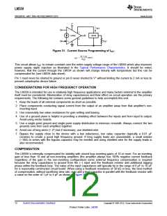
LM359
SNOSBT4C –MAY 1999–REVISED MARCH 2013
www.ti.com
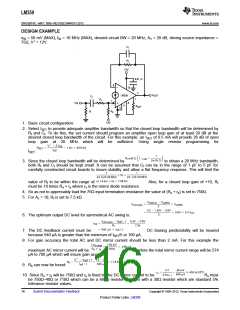
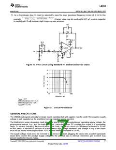
DESIGN EXAMPLE
eIN = 50 mV (MAX), fIN = 10 MHz (MAX), desired circuit BW = 20 MHz, AV = 20 dB, driving source impedance =
75Ω, V+ = 12V.
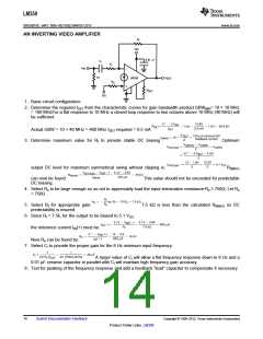
1. Basic circuit configuration:
2. Select ISET to provide adequate amplifier bandwidth so that the closed loop bandwidth will be determined by
Rf and Cf. To do this, the set current should program an amplifier open loop gain of at least 20 dB at the
desired closed loop bandwidth of the circuit. For this example, an ISET of 0.5 mA will provide 26 dB of open
loop gain at 20 MHz which will be sufficient. Using single resistor programming for
ISET
:
3. Since the closed loop bandwidth will be determined by
to obtain a 20 MHz bandwidth,
both Rf and Cf should be kept small. It can be assumed that Cf can be in the range of 1 pF to 5 pF for
carefully constructed circuit boards to insure stability and allow a flat frequency response. This will limit the
value of Rf to be within the range of:
Also, for a closed loop gain of +10, Rf
must be 10 times Rs + re where re is the mirror diode resistance.
4. So as not to appreciably load the 75Ω input termination resistance the value of (Rs + re) is set to 750Ω.
5. For Av = 10; Rf is set to 7.5 kΩ.
6. The optimum output DC level for symmetrical AC swing is:
7. The DC feedback current must be:
DC biasing predictability will be insured
because 640 μA is greater than the minimum of ISET/5 or 100 μA.
8. For gain accuracy the total AC and DC mirror current should be less than 2 mA. For this example the
maximum AC mirror current will be:
therefore the total mirror current range will be 574
μA to 706 μA which will insure gain accuracy.
9. Rb can now be found:
10. Since Rs + re will be 750Ω and re is fixed by the DC mirror current to be:
Rs must
be 750Ω–40Ω or 710Ω which can be a 680Ω resistor in series with a 30Ω resistor which are standard 5%
tolerance resistor values.
16
Submit Documentation Feedback
Copyright © 1999–2013, Texas Instruments Incorporated
Product Folder Links: LM359

 TI [ TEXAS INSTRUMENTS ]