LM359
SNOSBT4C –MAY 1999–REVISED MARCH 2013
www.ti.com
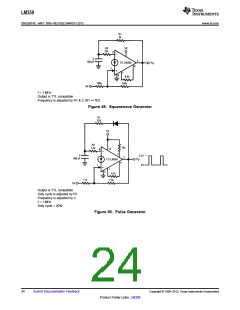
•
•
•
•
•
•
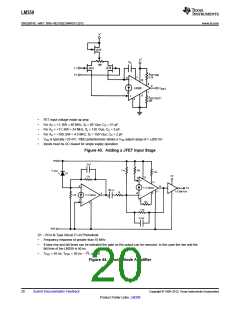
FET input voltage mode op amp
For AV = +1; BW = 40 MHz, Sr = 60 V/μs; CC = 51 pF
For AV = +11; BW = 24 MHz, Sr = 130 V/μs; CC = 5 pF
For AV = +100; BW = 4.5 MHz, Sr = 150 V/μs; CC = 2 pF
VOS is typically <25 mV; 100Ω potentiometer allows a VOS adjust range of ≈ ±200 mV
Inputs must be DC biased for single supply operation
Figure 43. Adding a JFET Input Stage
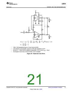
D1 ∼ RCA N-Type Silicon P-I-N Photodiode
•
•
Frequency response of greater than 10 MHz
If slow rise and fall times can be tolerated the gate on the output can be removed. In this case the rise and the
fall time of the LM359 is 40 ns.
•
TPDL = 45 ns, TPDH = 50 ns − T2L output
Figure 44. Photo Diode Amplifier
20
Submit Documentation Feedback
Copyright © 1999–2013, Texas Instruments Incorporated
Product Folder Links: LM359

 TI [ TEXAS INSTRUMENTS ]