LM359
SNOSBT4C –MAY 1999–REVISED MARCH 2013
www.ti.com
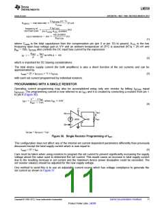
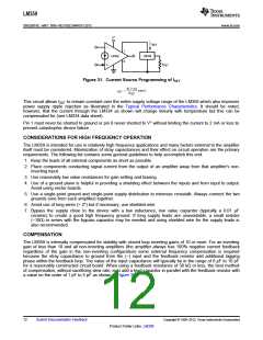
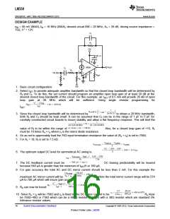
Figure 31. Current Source Programming of ISET
This circuit allows ISET to remain constant over the entire supply voltage range of the LM359 which also improves
power supply ripple rejection as illustrated in the Typical Performance Characteristics. It should be noted,
however, that the current through the LM334 as shown will change linearly with temperature but this can be
compensated for (see LM334 data sheet).
Pin 1 must never be shorted to ground or pin 8 never shorted to V+ without limiting the current to 2 mA or less to
prevent catastrophic device failure.
CONSIDERATIONS FOR HIGH FREQUENCY OPERATION
The LM359 is intended for use in relatively high frequency applications and many factors external to the amplifier
itself must be considered. Minimization of stray capacitances and their effect on circuit operation are the primary
requirements. The following list contains some general guidelines to help accomplish this end:
1. Keep the leads of all external components as short as possible.
2. Place components conducting signal current from the output of an amplifier away from that amplifier's non-
inverting input.
3. Use reasonably low value resistances for gain setting and biasing.
4. Use of a ground plane is helpful in providing a shielding effect between the inputs and from input to output.
Avoid using vector boards.
5. Use a single-point ground and single-point supply distribution to minimize crosstalk. Always connect the two
grounds (one from each amplifier) together.
6. Avoid use of long wires (> 2″) but if necessary, use shielded wire.
7. Bypass the supply close to the device with a low inductance, low value capacitor (typically a 0.01 μF
ceramic) to create a good high frequency ground. If long supply leads are unavoidable, a small resistor
(∼10Ω) in series with the bypass capacitor may be needed and using shielded wire for the supply leads is
also recommended.
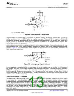
COMPENSATION
The LM359 is internally compensated for stability with closed loop inverting gains of 10 or more. For an inverting
gain of less than 10 and all non-inverting amplifiers (the amplifier always has 100% negative current feedback
regardless of the gain in the non-inverting configuration) some external frequency compensation is required
because the stray capacitance to ground from the (−) input and the feedback resistor add additional lagging
phase within the feedback loop. The value of the input capacitance will typically be in the range of 6 pF to 10 pF
for a reasonably constructed circuit board. When using a feedback resistance of 30 kΩ or less, the best method
of compensation, without sacrificing slew rate, is to add a lead capacitor in parallel with the feedback resistor with
a value on the order of 1 pF to 5 pF as shown in Figure 32.
12
Submit Documentation Feedback
Copyright © 1999–2013, Texas Instruments Incorporated
Product Folder Links: LM359

 TI [ TEXAS INSTRUMENTS ]