LM359
www.ti.com
SNOSBT4C –MAY 1999–REVISED MARCH 2013
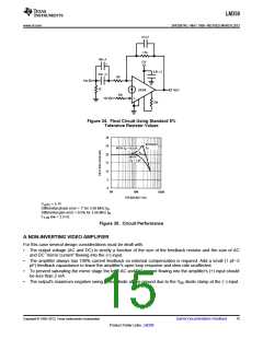
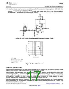
Figure 34. Final Circuit Using Standard 5%
Tolerance Resistor Values
Vo(DC) = 5.1V
Differential phase error < 1° for 3.58 MHz fIN
Differential gain error < 0.5% for 3.58 MHz fIN
f−3 dB low = 2.5 Hz
Figure 35. Circuit Performance
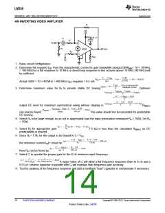
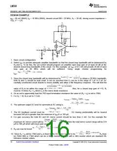
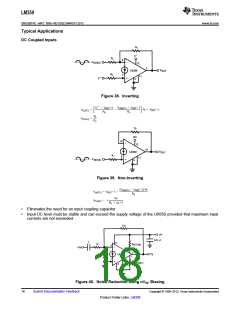
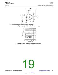
A NON-INVERTING VIDEO AMPLIFIER
For this case several design considerations must be dealt with.
•
•
•
•
The output voltage (AC and DC) is strictly a function of the size of the feedback resistor and the sum of AC
and DC “mirror current” flowing into the (+) input.
The amplifier always has 100% current feedback so external compensation is required. Add a small (1 pF–5
pF) feedback capacitance to leave the amplifier's open loop response and slew rate unaffected.
To prevent saturating the mirror stage the total AC and DC current flowing into the amplifier's (+) input should
be less than 2 mA.
The output's maximum negative swing is one diode above ground due to the VBE diode clamp at the (−) input.
Copyright © 1999–2013, Texas Instruments Incorporated
Submit Documentation Feedback
15
Product Folder Links: LM359

 TI [ TEXAS INSTRUMENTS ]