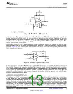
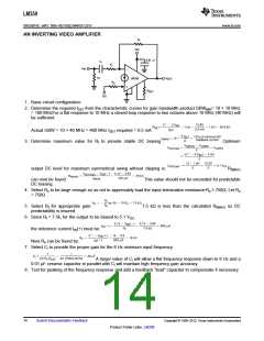
LM359
www.ti.com
SNOSBT4C –MAY 1999–REVISED MARCH 2013
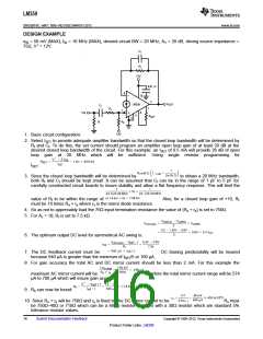
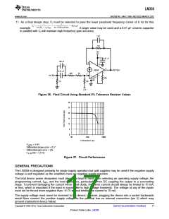
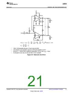
11. As a final design step, Ci must be selected to pass the lower passband frequency corner of 8 Hz for this
example. A larger value may be used and a 0.01 μF ceramic capacitor
in parallel with Ci will maintain high frequency gain accuracy.
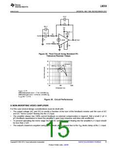
Figure 36. Final Circuit Using Standard 5% Tolerance Resistor Values
Vo(DC) = 5.4V
Differential phase error < 0.5°
Differential gain error < 2%
f−3 dB low = 2.5 Hz
Figure 37. Circuit Performance
GENERAL PRECAUTIONS
The LM359 is designed primarily for single supply operation but split supplies may be used if the negative supply
voltage is well regulated as the amplifiers have no negative supply rejection.
The total device power dissipation must always be kept in mind when selecting an operating supply voltage, the
programming current, ISET, and the load resistance, particularly when DC coupling the output to a succeeding
stage. To prevent damaging the current mirror input diode, the mirror current should always be limited to 10 mA,
or less, which is important if the input is susceptible to high voltage transients. The voltage at any of the inputs
must not be forced more negative than −0.7V without limiting the current to 10 mA.
The supply voltage must never be reversed to the device; however, plugging the device into a socket backwards
would then connect the positive supply voltage to the pin that has no internal connection (pin 5) which may
prevent inadvertent device failure.
Copyright © 1999–2013, Texas Instruments Incorporated
Submit Documentation Feedback
17
Product Folder Links: LM359

 TI [ TEXAS INSTRUMENTS ]