LM3410, LM3410Q
SNVS541G –OCTOBER 2007–REVISED MAY 2013
www.ti.com
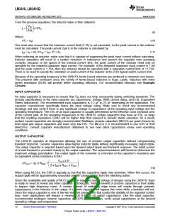
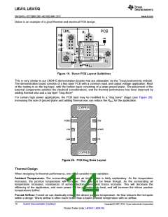
Below is an example of a good thermal and electrical PCB design.
LEDs
PCB
R1
PGND
DIM
FB
4
3
2
1
AGND
5
C2
VIN
VSW
6
VO
PGND
D1
C1
SW
L1
Figure 19. Boost PCB Layout Guidelines
This is very similar to our LM3410 demonstration boards that are obtainable via the Texas Instruments website.
The demonstration board consists of a two layer PCB with a common input and output voltage application. Most
of the routing is on the top layer, with the bottom layer consisting of a large ground plane. The placement of the
external components satisfies the electrical considerations, and the thermal performance has been improved by
adding thermal vias and a top layer “Dog-Bone”.
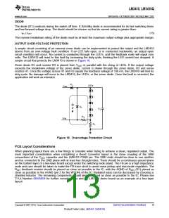
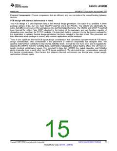
For certain high power applications, the PCB land may be modified to a "dog bone" shape (see Figure 20).
Increasing the size of ground plane and adding thermal vias can reduce the RθJA for the application.
COPPER
1
2
6
5
SW
PGND
VIN
AGND
3
4
FB
DIM
COPPER
Figure 20. PCB Dog Bone Layout
Thermal Design
When designing for thermal performance, one must consider many variables:
Ambient Temperature: The surrounding maximum air temperature is fairly explanatory. As the temperature
increases, the junction temperature will increase. This may not be linear though. As the surrounding air
temperature increases, resistances of semiconductors, wires and traces increase. This will decrease the
efficiency of the application, and more power will be converted into heat, and will increase the silicon junction
temperatures further.
Forced Airflow: Forced air can drastically reduce the device junction temperature. Air flow reduces the hot spots
within a design. Warm airflow is often much better than a lower ambient temperature with no airflow.
14
Submit Documentation Feedback
Copyright © 2007–2013, Texas Instruments Incorporated
Product Folder Links: LM3410 LM3410Q

 TI [ TEXAS INSTRUMENTS ]