LM3410, LM3410Q
www.ti.com
SNVS541G –OCTOBER 2007–REVISED MAY 2013
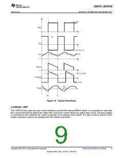
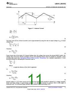
Di
I
( )
L t
L
i
L
V
IN
L
V
-V
OUT
IN
L
DT
S
T
S
t
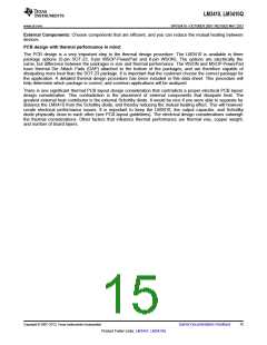
Figure 17. Inductor Current
V
≈
’
2DiL
DTS
IN
= ∆
÷
÷
∆
L
«
◊
V
≈
’
IN
x DT
∆
∆
÷
÷
Di =
L
S
2L
«
◊
(3)
The Duty Cycle (D) for a Boost converter can be approximated by using the ratio of output voltage (VOUT) to input
voltage (VIN).
VOUT
VIN
1
1
≈
’
=
=
∆
÷
Å
1 - D
D
«
◊
(4)
Therefore:
VOUT - VIN
VOUT
D =
(5)
Power losses due to the diode (D1) forward voltage drop, the voltage drop across the internal NMOS switch, the
voltage drop across the inductor resistance (RDCR) and switching losses must be included to calculate a more
accurate duty cycle (See Calculating Efficiency and Junction Temperature for a detailed explanation). A more
accurate formula for calculating the conversion ratio is:
h
VOUT
VIN
=
D‘
Where
•
η equals the efficiency of the LM3410 application.
(6)
(7)
(8)
Or:
VOUT x ILED
h =
VIN x IIN
Therefore:
VOUT - hVIN
D =
VOUT
Inductor ripple in a LED driver circuit can be greater than what would normally be allowed in a voltage regulator
Boost and Sepic design. A good design practice is to allow the inductor to produce 20% to 50% ripple of
maximum load. The increased ripple shouldn’t be a problem when illuminating LEDs.
Copyright © 2007–2013, Texas Instruments Incorporated
Submit Documentation Feedback
11
Product Folder Links: LM3410 LM3410Q

 TI [ TEXAS INSTRUMENTS ]