LM3410, LM3410Q
www.ti.com
SNVS541G –OCTOBER 2007–REVISED MAY 2013
DIODE
The diode (D1) conducts during the switch off time. A Schottky diode is recommended for its fast switching times
and low forward voltage drop. The diode should be chosen so that its current rating is greater than:
ID1 ≥ IOUT
(13)
The reverse breakdown rating of the diode must be at least the maximum output voltage plus appropriate margin.
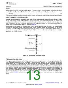
OUTPUT OVER-VOLTAGE PROTECTION
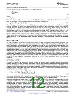
A simple circuit consisting of an external zener diode can be implemented to protect the output and the LM3410
device from an over-voltage fault condition. If an LED fails open, or is connected backwards, an output open
circuit condition will occur. No current is conducted through the LED’s, and the feedback node will equal zero
volts. The LM3410 will react to this fault by increasing the duty-cycle, thinking the LED current has dropped. A
simple circuit that protects the LM3410 is shown in Figure 18.
Zener diode D2 and resistor R3 is placed from VOUT in parallel with the string of LEDs. If the output voltage
exceeds the breakdown voltage of the zener diode, current is drawn through the zener diode, R3 and sense
resistor R1. Once the voltage across R1 and R3 equals the feedback voltage of 190 mV, the LM3410 will limit its
duty-cycle. No damage will occur to the LM3410, the LED’s, or the zener diode. Once the fault is corrected, the
application will work as intended.
D
1
LEDs
V
SW
O
V
P
D
2
C
2
R
3
V
FB
R
1
Figure 18. Overvoltage Protection Circuit
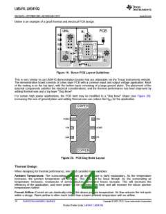
PCB Layout Considerations
When planning layout there are a few things to consider when trying to achieve a clean, regulated output. The
most important consideration when completing a Boost Converter layout is the close coupling of the GND
connections of the COUT capacitor and the LM3410 PGND pin. The GND ends should be close to one another
and be connected to the GND plane with at least two through-holes. There should be a continuous ground plane
on the bottom layer of a two-layer board except under the switching node island. The FB pin is a high impedance
node and care should be taken to make the FB trace short to avoid noise pickup and inaccurate regulation. The
RSET feedback resistor should be placed as close as possible to the IC, with the AGND of RSET (R1) placed as
close as possible to the AGND (pin 5 for the WSON) of the IC. Radiated noise can be decreased by choosing a
shielded inductor. The remaining components should also be placed as close as possible to the IC. Please see
TI Lit Number SNVA054 for further considerations and the LM3410 demo board as an example of a four-layer
layout.
Copyright © 2007–2013, Texas Instruments Incorporated
Submit Documentation Feedback
13
Product Folder Links: LM3410 LM3410Q

 TI [ TEXAS INSTRUMENTS ]