LM3410, LM3410Q
SNVS541G –OCTOBER 2007–REVISED MAY 2013
www.ti.com
APPLICATION INFORMATION
THEORY OF OPERATION
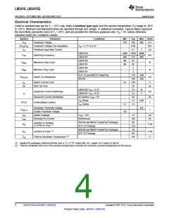
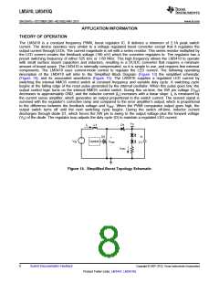
The LM3410 is a constant frequency PWM, boost regulator IC. It delivers a minimum of 2.1A peak switch
current. The device operates very similar to a voltage regulated boost converter except that it regulates the
output current through LEDs. The current magnitude is set with a series resistor. This series resistor multiplied by
the LED current creates the feedback voltage (190 mV) which the converter regulates to. The regulator has a
preset switching frequency of either 525 kHz or 1.60 MHz. This high frequency allows the LM3410 to operate
with small surface mount capacitors and inductors, resulting in a DC/DC converter that requires a minimum
amount of board space. The LM3410 is internally compensated, so it is simple to use, and requires few external
components. The LM3410 uses current-mode control to regulate the LED current. The following operating
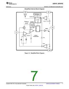
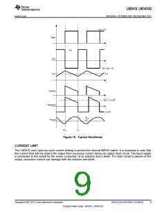
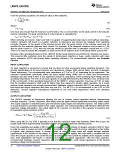
description of the LM3410 will refer to the Simplified Block Diagram (Figure 13) the simplified schematic
(Figure 14), and its associated waveforms (Figure 15). The LM3410 supplies a regulated LED current by
switching the internal NMOS control switch at constant frequency and variable duty cycle. A switching cycle
begins at the falling edge of the reset pulse generated by the internal oscillator. When this pulse goes low, the
output control logic turns on the internal NMOS control switch. During this on-time, the SW pin voltage (VSW
)
decreases to approximately GND, and the inductor current (IL) increases with a linear slope. IL is measured by
the current sense amplifier, which generates an output proportional to the switch current. The sensed signal is
summed with the regulator’s corrective ramp and compared to the error amplifier’s output, which is proportional
to the difference between the feedback voltage and VREF. When the PWM comparator output goes high, the
output switch turns off until the next switching cycle begins. During the switch off-time, inductor current
discharges through diode D1, which forces the SW pin to swing to the output voltage plus the forward voltage
(VD) of the diode. The regulator loop adjusts the duty cycle (D) to maintain a regulated LED current.
V
O
I
L1
D1
L
I
Q1
C
+
V
IN
Control
V
SW
-
C1
I
LED
Figure 14. Simplified Boost Topology Schematic
8
Submit Documentation Feedback
Copyright © 2007–2013, Texas Instruments Incorporated
Product Folder Links: LM3410 LM3410Q

 TI [ TEXAS INSTRUMENTS ]