LM26420, LM26420-Q0, LM26420-Q1
www.ti.com
SNVS579J –FEBRUARY 2009–REVISED SEPTEMBER 2015
7 Detailed Description
7.1 Overview
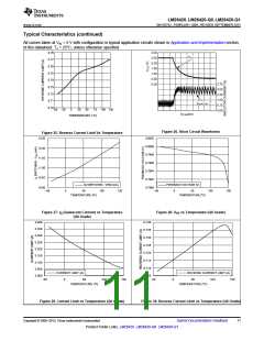
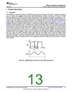
The LM26420 is a constant frequency dual PWM buck synchronous regulator device that can supply two loads at
up to 2 A each. The regulator has a preset switching frequency of either 2.2 MHz or 550 kHz. This high
frequency allows the LM26420 to operate with small surface mount capacitors and inductors, resulting in a DC-
DC converter that requires a minimum amount of board space. The LM26420 is internally compensated, so it is
simple to use and requires few external components. The LM26420 uses current-mode control to regulate the
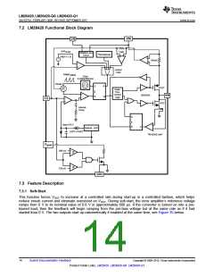
output voltage. The following operating description of the LM26420 will refer to the LM26420 Functional Block
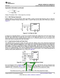
Diagram, which depicts the functional blocks for one of the two channels, and to the waveforms in Figure 34. The
LM26420 supplies a regulated output voltage by switching the internal PMOS and NMOS switches at constant
frequency and variable duty cycle. A switching cycle begins at the falling edge of the reset pulse generated by
the internal clock. When this pulse goes low, the output control logic turns on the internal PMOS control switch
(TOP Switch). During this on-time, the SW pin voltage (VSW) swings up to approximately VIN, and the inductor
current (IL) increases with a linear slope. IL is measured by the current sense amplifier, which generates an
output proportional to the switch current. The sense signal is summed with the regulator’s corrective ramp and
compared to the error amplifier’s output, which is proportional to the difference between the feedback voltage
and VREF. When the PWM comparator output goes high, the TOP Switch turns off and the NMOS switch
(BOTTOM Switch) turns on after a short delay, which is controlled by the Dead-Time-Control Logic, until the next
switching cycle begins. During the top switch off-time, inductor current discharges through the BOTTOM Switch,
which forces the SW pin to swing to ground. The regulator loop adjusts the duty cycle (D) to maintain a constant
output voltage.
V
SW
D = T /T
ON SW
V
IN
SW
Voltage
T
T
OFF
ON
0
t
T
SW
I
L
I
PK
Inductor
Current
0
t
Figure 34. LM26420 Basic Operation of the PWM Comparator
Copyright © 2009–2015, Texas Instruments Incorporated
Submit Documentation Feedback
13
Product Folder Links: LM26420 LM26420-Q0 LM26420-Q1

 TI [ TEXAS INSTRUMENTS ]