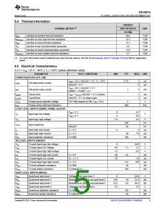
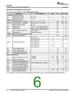
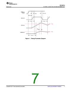
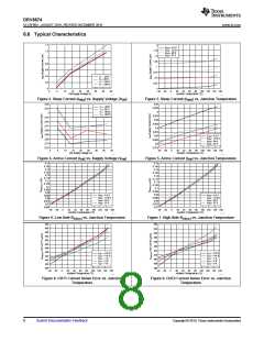
DRV8874
www.ti.com
SLVSF66A –AUGUST 2019–REVISED DECEMBER 2019
7 Detailed Description
7.1 Overview
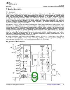
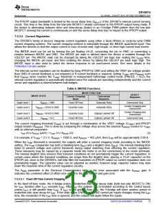
The DRV887x family of devices are brushed DC motor drivers that operate from 4.5 to 37-V supporting a wide
range of output load currents for various types of motors and loads. The devices integrate an H-bridge output
power stage that can be operated in different control modes set by the PMODE pin setting. This allows for driving
a single bidirectional brushed DC motor, two unidirectional brushed DC motors, or other output load
configurations. The devices integrate a charge pump regulator to support more efficient high-side N-channel
MOSFETs and 100% duty cycle operation. The devices operate from a single power supply input (VM) which can
be directly connected to a battery or DC voltage supply. The nSLEEP pin provides an ultra-low power mode to
minimize current draw during system inactivity.
The DRV887x family of devices also integrate current sense output using current mirrors on the low-side power
MOSFETs. The IPROPI pin sources a small current that is proportional to the current in the MOSFETs. This
current can be converted to a proportional voltage using an external resistor (RIPROPI). The integrated current
sensing allows the DRV887x devices to limit the output current with a fixed off-time PWM chopping scheme and
provide load information to the external controller to detect changes in load or stall conditions. The integrated
current sensing outperforms traditional external shunt resistor sensing by providing current information even
during the off-time slow decay recirculating period and removing the need for an external power shunt resistor.
The off-time PWM current regulation level can be configured during motor operation through the VREF pin to
limit the load current accordingly to the system demands.
A variety of integrated protection features protect the device in the case of a system fault. These include
undervoltage lockout (UVLO), charge pump undervoltage (CPUV), overcurrent protection (OCP), and
overtemperature shutdown (TSD). Fault conditions are indicated on the nFAULT pin.
7.2 Functional Block Diagram
VM
VM
VM
Gate Driver
VVCP
0.1 …F
VVCP
VCP
CPH
CPL
GND
0.1 …F
VCP
Charge
Pump
HS
OUT1
VDD
0.022 …F
LS
VDD
Internal
Regulator
ISEN1
VM
Power
Digital
Core
Gate Driver
VVCP
nSLEEP
EN/IN1
PH/IN2
HS
OUT2
PGND
VDD
Control
Inputs
LS
PMODE
IMODE
3-Level
VVCC
4-Level
ISEN2
VVCC
RPU
VREF
Fault Output
+
nFAULT
IPROPI
Clamp
œ
ISEN1
ISEN2
IPROPI
Current
Sense
RIPROPI
Copyright © 2019, Texas Instruments Incorporated
Submit Documentation Feedback
9

 TI [ TEXAS INSTRUMENTS ]