DRV8874
SLVSF66A –AUGUST 2019–REVISED DECEMBER 2019
www.ti.com
7.3 Feature Description
7.3.1 External Components
Table 1 lists the recommended external components for the device.
Table 1. Recommended External Components
COMPONENT
CVM1
PIN 1
VM
PIN 2
GND
RECOMMENDED
0.1-µF, low ESR ceramic capacitor, VM-rated.
Bulk Capacitance, VM-rated.
CVM2
VM
VCP
GND
VM
CVCP
X5R or X7R, 100-nF, 16-V ceramic capacitor
X5R or X7R, 22-nF, VM-rated ceramic capacitor
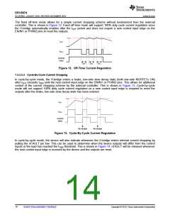
See Current Regulation.
CFLY
CPH
CPL
RIMODE
RPMODE
RnFAULT
RIPROPI
IMODE
PMODE
VCC
GND
GND
nFAULT
GND
See Control Modes.
Pullup resistor, IOD ≤ 5-mA
IPROPI
See Current Sensing.
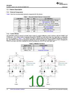
7.3.2 Control Modes
The DRV887x family of devices provides three modes to support different control schemes with the EN/IN1 and
PH/IN2 pins. The control mode is selected through the PMODE pin with either logic low, logic high, or setting the
pin Hi-Z as shown in Table 2. The PMODE pin state is latched when the device is enabled through the nSLEEP
pin. The PMODE state can be changed by taking the nSLEEP pin logic low, waiting the tSLEEP time, changing the
PMODE pin input, and then enabling the device by taking the nSLEEP pin back logic high.
Table 2. PMODE Functions
PMODE STATE
PMODE = Logic Low
PMODE = Logic High
PMODE = Hi-Z
CONTROL MODE
PH/EN
PWM
Independent Half-Bridge
VM
VM
1
22
3
1
2
3
Reverse drive
Forward drive
Slow decay (brake)
High-Z (coast)
Slow decay (brake)
High-Z (coast)
1
1
OUT1
OUT2
OUT1
OUT2
2
2
3
3
Forward
Reverse
Figure 10. H-Bridge States
10
Submit Documentation Feedback
Copyright © 2019, Texas Instruments Incorporated

 TI [ TEXAS INSTRUMENTS ]