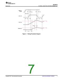
DRV8874
SLVSF66A –AUGUST 2019–REVISED DECEMBER 2019
www.ti.com
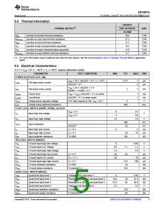
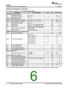
Electrical Characteristics (continued)
4.5 V ≤ VVM ≤ 37 V, –40°C ≤ TJ ≤ 150°C (unless otherwise noted)
PARAMETER
TEST CONDITIONS
MIN
TYP
MAX
UNIT
OPEN-DRAIN OUTPUTS (nFAULT)
VOL
IOZ
Output logic low voltage
Output logic high current
IOD = 5 mA
VOD = 5 V
0.3
2
V
–2
µA
DRIVER OUTPUTS (OUT1, OUT2)
RDS(on)_HS
RDS(on)_LS
VSD
High-side MOSFET on resistance
VVM = 24 V, IO = 2 A, TJ = 25°C
VVM = 24 V, IO = –2 A, TJ = 25°C
ISD = 1 A
100
100
0.9
120
120
mΩ
mΩ
V
Low-side MOSFET on resistance
Body diode forward voltage
Output rise time
tRISE
VVM = 24 V, OUTx rising 10% to 90%
VVM = 24 V, OUTx falling 90% to 10%
150
150
ns
tFALL
Output fall time
ns
EN/IN1, PH/IN2 to OUTx, 200 Ω from
OUTx to GND
tPD
Input to output propagation delay
Output dead time
400
100
ns
ns
tDEAD
Body diode conducting
CURRENT SENSE AND REGULATION (IPROPI, VREF)
AIPROPI
Current mirror scaling factor
450
µA/A
mA
IOUT < 0.4 A
5.5 V ≤ VVM ≤ 37 V
–30
–7.5
–6
30
7.5
6
0.4 A ≤ IOUT < 1 A
5.5 V ≤ VVM ≤ 37 V
(1)
AERR
Current mirror scaling error
1 A ≤ IOUT < 2 A
5.5 V ≤ VVM ≤ 37 V
%
2 A ≤ IOUT ≤ 4 A
5.5 V ≤ VVM ≤ 37 V
–5.5
5.5
tOFF
Current regulation off time
Current sense delay time
25
1.6
0.6
1.1
µs
µs
µs
µs
tDELAY
tDEG
tBLK
Current regulation deglitch time
Current regulation blanking time
PROTECTION CIRCUITS
VVM rising
VVM falling
4.3
4.2
4.45
4.35
100
10
4.6
4.5
V
V
VUVLO
Supply undervoltage lockout (UVLO)
VUVLO_HYS
tUVLO
VCPUV
IOCP
Supply UVLO hysteresis
mV
µs
V
Supply undervoltage deglitch time
Charge pump undervoltage lockout
Overcurrent protection trip point
Overcurrent protection deglitch time
Overcurrent protection retry time
Thermal shutdown temperature
Thermal shutdown hysteresis
VCP with respect to VM, VVCP falling
2.25
10
6
A
tOCP
3
µs
ms
°C
°C
tRETRY
TTSD
2
160
175
20
190
THYS
(1) At low currents, the IPROPI output has a fixed offset error with respect to the IOUT current through the low-side power MOSFETs.
6
Submit Documentation Feedback
Copyright © 2019, Texas Instruments Incorporated

 TI [ TEXAS INSTRUMENTS ]