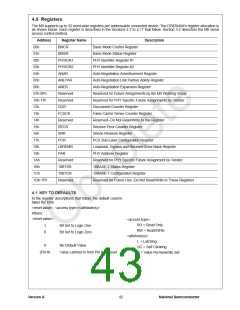
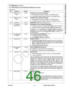
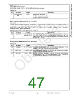
4.0 Registers
The MII supports up to 32 word-wide registers per addressable connected device. The DP83840A's register allocation is
as shown below. Each register is described in the Sections 4.2 to 4.17 that follow. Section 3.2 describes the MII serial
access control method.
Address
00h
Register Name
BMCR
Description
Basic Mode Control Register
Basic Mode Status Register
PHY Identifier Register #1
PHY Identifier Register #2
01h
BMSR
02h
PHYIDR1
PHYIDR2
ANAR
03h
04h
Auto-Negotiation Advertisement Register
Auto-Negotiation Link Partner Ability Register
Auto-Negotiation Expansion Register
05h
ANLPAR
ANER
06h
07h-0Fh
10h-11h
12h
Reserved
Reserved
DCR
Reserved for Future Assignments by the MII Working Group
Reserved for PHY Specific Future Assignments by Vendor
Disconnect Counter Register
13h
FCSCR
Reserved
RECR
False Carrier Sense Counter Register
14h
Reserved--Do Not Read/Write to this Register
Receive Error Counter Register
15h
16h
SRR
Silicon Revision Register
17h
PCR
PCS Sub-Layer Configuration Register
Loopback, Bypass and Receiver Error Mask Register
PHY Address Register
18h
LBREMR
PAR
19h
1Ah
Reserved
10BTSR
10BTCR
Reserved
Reserved for PHY Specific Future Assignment by Vendor
10BASE-T Status Register
1Bh
1Ch
1Dh-1Fh
10BASE-T Configuration Register
Reserved for Future Use--Do Not Read/Write to These Registers
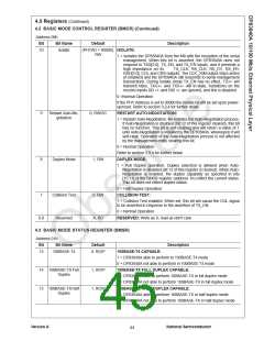
4.1 KEY TO DEFAULTS
In the register descriptions that follow, the default column
takes the form
<reset value>, <access type>/<attribute(s)>
Where:
<reset value>:
<access type>:
RO = Read Only
RW = Read/Write
<attribute(s)>:
1
0
Bit Set to Logic One
Bit Set to Logic Zero
L = Latching
X
No Default Value
SC = Self Clearing
P = Value Permanently Set
(Pin #)
Value Latched in from Pin # at Reset
Version A
42
National Semiconductor

 TI [ TEXAS INSTRUMENTS ]