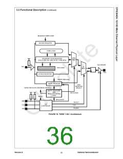
3.0 Functional Description (Continued)
3.9.6 Auto-Negotiation Complete Time
of the device. In this case, it is recommended that a
positive pulse, with a duration of at least 1µs, be applied to
the RESET pin no sooner than 500µs after the point in time
where the initial VCC ramp reached 4V.
This section describes the amount of time required to
complete an Auto-Negotiation cycle for the 840A. These
times are defined for two cases. The first case assumes
that the far end link partner does not support Auto-
In both methods described above, it is important to note
that the logic levels present at each of the hardware
configuration pins of the DP83840A (see list below) are
also latched into the device as a function of the reset
operation (either hardware or software). These hardware
configuration values are guaranteed to be latched into the
DP83840A 2µs after the deassertion of the RESET pin.
Negotiation and is either
implementation.
a
fixed 10M or 100M
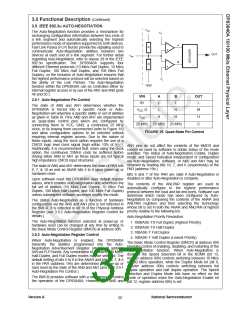
Timer
Min spec
1200ms
500ms
Max spec
1500ms
1000ms
1000ms
840A
break link
autoneg wait
link fail inhibit
1300ms
750ms
800ms
750ms
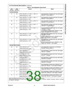
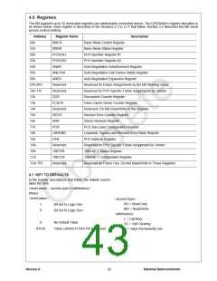
The hardware configuration values latched into the
DP83840A during the reset operation are dependent on
the logic levels present at the following device pins upon
power-up:
------------------------------------------------------------------------------
Total 1700-2450ms 2500-3500ms
2050-2850ms
The second case assumes that the far end link partner fully
supports Auto-Negotiation:
Pin #
49
53
66
89
63
95
46
47
98
99
100
1
Primary Function
LBEN
Latched in at Reset
PHYAD[0]
PHYAD[1]
PHYAD[2]
PHYAD[3]
PHYAD[4]
AN0
Timer
Min spec
1200ms
104ms
Max spec
1500ms
312ms
840A
break link
FLP bursts
link fail inhibit
1300ms
200ms
800ms
ENCSEL
CRS
750ms
1000ms
------------------------------------------------------------------------------
Total 1304-2054ms 1812-2812ms
PHYAD[3]
RX_ER
1500-2300ms
Refer to chapter 28 of the IEEE 802.3u standard for a full
description of the individual timers related to Auto-
Negotiation.
AN0
AN1
AN1
3.10 RESET OPERATION
REPEATER
10BTSER
BPALIGN
BP4B5B
BPSCR
REPEATER
10BTSER
BPALIGN
BP4B5B
The DP83840A can be reset either by hardware or
software. A hardware reset may be accomplished either by
asserting the RESET pin (pin 44) during normal operation,
or upon powering up the device. A software reset is
accomplished by setting the reset bit in the Basic Mode
Control Register (bit 15, address 00h).
BPSCR
While either the hardware or software reset can be
implemented at any time after device initialization,
providing a hardware reset, as described in section
3.10.1, must be implemented upon device power-up/
initialization. Omitting the hardware reset operation
during the device power-up/initialization sequence can
result in improper device operation.
During the power-up reset operation the LED1 through
LED5 pins are undefined, the SPEED_10 pin will be
asserted, and the SPEED_100 pin will be deasserted.
3.10.2 Hardware Reset
A hardware Reset is accomplished by applying a positive
pulse, with a duration of at least 1 µs, to the RESET pin of
the DP83840A during normal operation. This will reset the
device such that all registers will be reset to default values
and the hardware configuration values will be re-latched
into the device (similar to the power-up reset operation).
3.10.1 Power-up / Reset
When VCC is first applied to the DP83840A it takes some
amount of time for power to actually reach the nominal 5V
potential. This initial power-up time can be referred to as a
V
CC ramp when VCC is “ramping” from 0V to 5V. When the
3.10.3 Software Reset
initial VCC ramp reaches approximately 4V, the DP83840A
begins an internal reset operation which must be allowed A software reset is accomplished by setting bit 15 of the
sufficient time, relative to the assertion and deassertion of Basic Mode Control Register (address 00h). This bit is self
the RESET pin, to reset the device. There are two methods clearing and, when set, will return a value of “1” until the
for guaranteeing successful reset upon device power-up.
software reset operation has completed. The software
reset will reset the device such that all registers will be
reset to default values and the hardware configuration
values will be re-latched into the device (similar to the
power-up reset operation). Driver code should wait 500µs
following a software reset before allowing further serial MII
operations with the DP83840A.
The first method accounts for those designs that utilize a
special power up circuit which, through hardware, will
assert the RESET pin upon power-up. In this case, the
deassertion (falling edge) of the RESET pin must not occur
until at least 500µs after the time at which the VCC ramp
initially reached the 4V point.
The second method accounts for those applications which
produce a reset pulse sometime after the initial power-up
Version A
National Semiconductor
39

 TI [ TEXAS INSTRUMENTS ]