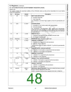
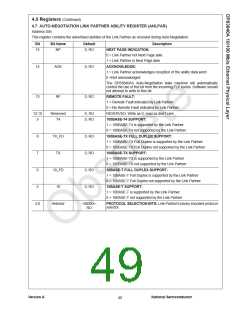
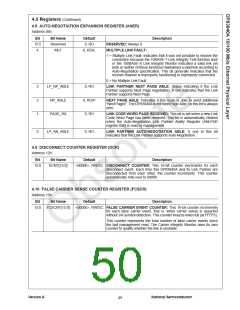
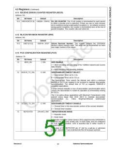
4.0 Registers (Continued)
4.3 BASIC MODE STATUS REGISTER (BMSR) (Continued)
Address 01h
Bit
Bit Name
Default
Description
0
Extended Capa-
bility
1, RO/P
EXTENDED CAPABILITY:
1 = Extended register capable
0 = Basic register capable only
4.4 PHY IDENTIFIER REGISTER #1 (PHYIDR1)
Address 02h
The PHY Identifier Registers #1 and #2 together form a unique identifier for the DP83840A. The Identifier consists of a
concatenation of the Organizationally Unique Identifier (OUI), the vendor's model number and the model revision
number. A PHY may return a value of zero in each of the 32 bits of the PHY Identifier if desired. The PHY Identifier is
intended to support network management.
National Semiconductor's IEEE assigned OUI is 080017h.
Bit
Bit Name
Default
Description
15:0
OUI_MSB
<00 1000 0000 OUI MOST SIGNIFICANT BITS: This register stores bits 3 to 18 of the
OUI (080017h) to bits 15 to 0 of this register respectively. The most
significant two bits of the OUI are ignored (the IEEE standard refers to
these as bits 1 and 2).
0000 00>, RO/P
4.5 PHY IDENTIFIER REGISTER #2 (PHYIDR2)
Address 03h
Bit
Bit Name
Default
Description
15:10
OUI_LSB
<01 0111>, RO/P OUI LEAST SIGNIFICANT BITS: Bits 19 to 24 of the OUI (080017h) are
mapped to bits 15 to 10 of this register respectively.
9:4
3:0
VNDR_MDL
MDL_REV
<00 0000>, RO/P VENDOR MODEL NUMBER: Six bits of vendor model number mapped
to bits 9 to 4 (most significant bit to bit 9).
<0001>, RO/P
MODEL REVISION NUMBER: Four bits of vendor model revision
number mapped to bits 3 to 0 (most significant bit to bit 3). This field will
be incremented for all major DP83840A device changes.
Version A
National Semiconductor
46

 TI [ TEXAS INSTRUMENTS ]