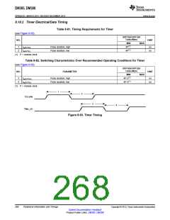
DM385, DM388
SPRS821D –MARCH 2013–REVISED DECEMBER 2013
www.ti.com
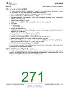
8.20.2 USB2.0 Electrical Data/Timing
Table 8-85. Switching Characteristics Over Recommended Operating Conditions for USB2.0
(see Figure 8-95)
OPP100/OPP120/
Turbo/Nitro
NO.
PARAMETER
LOW SPEED
1.5 Mbps
FULL SPEED
12 Mbps
HIGH SPEED
480 Mbps
UNIT
MIN
75
MAX
MIN
4
MAX
20
20
111
2
MIN
0.5
0.5
–
MAX
1
2
3
4
5
tr(D)
Rise time, USBx_DP and USBx_DM signals(1)
Fall time, USBx_DP and USBx_DM signals(1)
Rise/Fall time, matching(2)
300
300
125
2
ns
ns
%
tf(D)
75
4
trfM
80
90
1.3
–
VCRS
Output signal cross-over voltage(1)
Source (Host) Driver jitter, next transition
Function Driver jitter, next transition
Source (Host) Driver jitter, paired transition(4)
Function Driver jitter, paired transition
Pulse duration, EOP transmitter
Pulse duration, EOP receiver(5)
Data Rate
1.3
–
–
(3)
V
tjr(source)NT
tjr(FUNC)NT
tjr(source)PT
tjr(FUNC)PT
tw(EOPT)
tw(EOPR)
t(DRATE)
2
2
ns
ns
ns
ns
ns
ns
(3)
(3)
(3)
25
2
6
1
1
10
1
7
8
9
1250
670
1500
160
82
175
–
–
–
1.5
–
12
49.5
–
480 Mb/s
10 ZDRV
11 ZINP
Driver Output Resistance
–
28
40.5
–
49.5
–
Ω
Receiver Input Impedance
300
300
kΩ
(1) Low Speed: CL = 200 pF, Full Speed: CL = 50 pF, High Speed: CL = 50 pF
(2) tRFM = (tr/tf) x 100. [Excluding the first transaction from the Idle state.]
(3) For more detailed information, see the Universal Serial Bus Specification Revision 2.0, Chapter 7, Electrical.
(4) tjr = tpx(1) - tpx(0)
(5) Must accept as valid EOP.
t
t
per − jr
USBx_DM
V
90% V
OH
CRS
10% V
OL
USBx_DP
t
f
t
r
Figure 8-95. USB2.0 Integrated Transceiver Interface Timing
For more detailed information on USB2.0 board design, routing, and layout guidelines, see the USB 2.0
Board Design and Layout Guidelines Application Report (Literature Number: SPRAAR7).
272
Peripheral Information and Timings
Copyright © 2013, Texas Instruments Incorporated
Submit Documentation Feedback
Product Folder Links: DM385 DM388

 TI [ TEXAS INSTRUMENTS ]