DM385, DM388
SPRS821D –MARCH 2013–REVISED DECEMBER 2013
www.ti.com
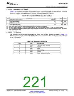
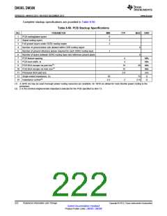
Complete stackup specifications are provided in Table 8-50.
Table 8-50. PCB Stackup Specifications
NO.
1
PARAMETER
MIN
6
TYP
MAX
UNIT
PCB routing/plane layers
Signal routing layers
2
3
3
Full ground layers under DDR2 routing region
Number of ground plane cuts allowed within DDR routing region
Number of ground reference planes required for each DDR2 routing layer
Number of layers between DDR2 routing layer and reference ground plane
PCB feature spacing
2
4
0
0
5
1
6
7
4
4
Mils
Mils
Mils
Mils
mm
Ω
8
PCB trace width, w
PCB BGA escape via pad size(1)
9
18
10
0.4
20
10 PCB BGA escape via hole size(1)
11 Processor BGA pad size
13 Single-ended impedance, Zo
14 Impedance control(2)
50
75
Z-5
Z
Z+5
Ω
(1) A 20/10 via may be used if enough power routing resources are available. An 18/10 via allows for more flexible power routing to the
processor.
(2) Z is the nominal singled-ended impedance selected for the PCB specified by item 13.
222
Peripheral Information and Timings
Copyright © 2013, Texas Instruments Incorporated
Submit Documentation Feedback
Product Folder Links: DM385 DM388

 TI [ TEXAS INSTRUMENTS ]