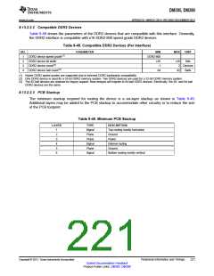
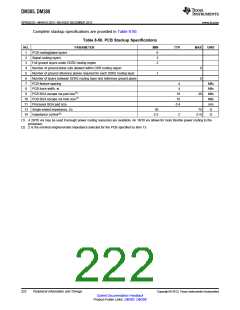
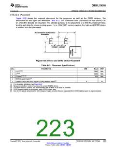
DM385, DM388
www.ti.com
NO.
SPRS821D –MARCH 2013–REVISED DECEMBER 2013
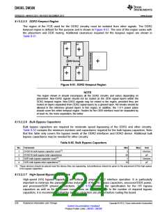
Table 8-53. High-Speed Bypass Capacitors
PARAMETER
MIN
MAX
UNIT
1
2
3
4
5
6
7
8
9
HS bypass capacitor package size(1)
0402 10 Mils
Distance from HS bypass capacitor to device being bypassed
Number of connection vias for each HS bypass capacitor(2)
Trace length from bypass capacitor contact to connection via
Number of connection vias for each processor power/ground ball
Trace length from processor power/ground ball to connection via
Number of connection vias for each DDR2 device power/ground ball
Trace length from DDR2 device power/ground ball to connection via
DVDD18 HS bypass capacitor count(3)
250
30
Mils
Vias
Mils
2
1
1
Vias
Mils
35
1
Vias
Mils
35
20
1.2
8
Devices
μF
10 DVDD18 HS bypass capacitor total capacitance
11 DDR device HS bypass capacitor count(4)(5)
12 DDR device HS bypass capacitor total capacitance(5)
Devices
μF
0.4
(1) LxW, 10-mil units, that is, a 0402 is a 40x20-mil surface-mount capacitor.
(2) An additional HS bypass capacitor can share the connection vias only if it is mounted on the opposite side of the board.
(3) These devices should be placed as close as possible to the device being bypassed.
(4) These devices should be placed as close as possible to the device being bypassed.
(5) Per DDR device.
8.13.2.2.8 Net Classes
Table 8-54 lists the clock net classes for the DDR2 interface. Table 8-55 lists the signal net classes, and
associated clock net classes, for the signals in the DDR2 interface. These net classes are used for the
termination and routing rules that follow.
Table 8-54. Clock Net Class Definitions
CLOCK NET CLASS PROCESSOR PIN NAMES
CK
DDR[0]_CLK/DDR[0]_CLK
DQS0
DDR[0]_DQS[0]/DDR[0]_DQS[0]
DDR[0]_DQS[1]/DDR[0]_DQS[1]
DDR[0]_DQS[2]/DDR[0]_DQS[2]
DDR[0]_DQS[3]/DDR[0]_DQS[3]
DQS1
DQS2(1)
DQS3(1)
(1) Only used on 32-bit wide DDR2 memory systems.
Copyright © 2013, Texas Instruments Incorporated
Peripheral Information and Timings
225
Submit Documentation Feedback
Product Folder Links: DM385 DM388

 TI [ TEXAS INSTRUMENTS ]