DM385, DM388
SPRS821D –MARCH 2013–REVISED DECEMBER 2013
www.ti.com
8.13.1 DDR2/3/3L Memory Controller Register Descriptions
The DDR2/3/3L peripheral registers are described in the device-specific Technical Reference Manual.
Each register is documented as an offset from a base address for the peripheral. The base addresses for
all of the peripherals are in the device memory map (see Section 2.10).
8.13.2 DDR2 Routing Specifications
8.13.2.1 Board Designs
TI only supports board designs that follow the guidelines outlined in this document. The switching
characteristics and the timing diagram for the DDR2 memory controller are shown in Table 8-47 and
Figure 8-47.
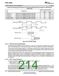
Table 8-47. Switching Characteristics Over Recommended Operating Conditions for DDR2 Memory
Controller
-1G
NO.
PARAMETER
UNIT
MIN
MAX
1
tc(DDR_CLK)
Cycle time, DDR_CLK
2.5
8
ns
1
DDR_CLK
Figure 8-47. DDR2 Memory Controller Clock Timing
8.13.2.2 DDR2 Interface
This section provides the timing specification for the DDR2 interface as a PCB design and manufacturing
specification. The design rules constrain PCB trace length, PCB trace skew, signal integrity, cross-talk,
and signal timing. These rules, when followed, result in a reliable DDR2 memory system without the need
for a complex timing closure process. For more information regarding the guidelines for using this DDR2
specification, see the Understanding TI’s PCB Routing Rule-Based DDR Timing Specification Application
Report (Literature Number: SPRAAV0).
8.13.2.2.1 DDR2 Interface Schematic
Figure 8-48 shows the DDR2 interface schematic for a x32 DDR2 memory system. In Figure 8-49 the x16
DDR2 system schematic is identical except that the high-word DDR2 device is deleted.
When not using a DDR2 interface, the proper method of handling the unused pins is to tie off the DQS
pins by pulling the non-inverted DQS pin to the DVDD_DDR[0] supply via a 1k-Ω resistor and pulling the
inverted DQS pin to ground via a 1k-Ω resistor. This needs to be done for each byte not used. Also,
include the 50-Ω pulldown for DDR[0]_VTP. The DVDD_DDR[0] and VREFSSTL_DDR[0] power supply
pins must be connected to their respective power supplies even if DDR[0] is not used. All other DDR
interface pins can be left unconnected. Note that the supported modes for use of the DDR EMIF are 32-
bits wide, 16-bits wide, or not used.
218
Peripheral Information and Timings
Copyright © 2013, Texas Instruments Incorporated
Submit Documentation Feedback
Product Folder Links: DM385 DM388

 TI [ TEXAS INSTRUMENTS ]