DM385, DM388
SPRS821D –MARCH 2013–REVISED DECEMBER 2013
www.ti.com
Table 8-55. Signal Net Class Definitions
ASSOCIATED CLOCK
CLOCK NET CLASS
PROCESSOR PIN NAMES
NET CLASS
ADDR_CTRL
CK
DDR[0]_BA[2:0], DDR[0]_A[15:0], DDR[0]_CS[x], DDR[0]_CAS,
DDR[0]_RAS, DDR[0]_WE, DDR[0]_CKE, DDR[0]_ODT[0]
DQ0
DQ1
DQ2(1)
DQ3(1)
DQS0
DQS1
DQS2
DQS3
DDR[0]_D[7:0], DDR[0]_DQM[0]
DDR[0]_D[15:8], DDR[0]_DQM[1]
DDR[0]_D[23:16], DDR[0]_DQM[2]
DDR[0]_D[31:24], DDR[0]_DQM[3]
(1) Only used on 32-bit wide DDR2 memory systems.
8.13.2.2.9 DDR2 Signal Termination
Signal terminators are required in CK and ADDR_CTRL net classes. Serial terminators may be used on
data lines to reduce EMI risk; however, serial terminations are the only type permitted. ODT's are
integrated on the data byte net classes. They should be enabled to ensure signal integrity.Table 8-56
shows the specifications for the series terminators.
Table 8-56. DDR2 Signal Terminations
NO.
1
PARAMETER
MIN
0
TYP
MAX UNIT
CK net class(1)(2)
ADDR_CTRL net class(1) (2)(3)(4)
10
Zo
Zo
Ω
Ω
Ω
2
0
22
3
Data byte net classes (DQS0-DQS3, DQ0-DQ3)(5)
0
(1) Only series termination is permitted, parallel or SST specifically disallowed on board.
(2) Only required for EMI reduction.
(3) Terminator values larger than typical only recommended to address EMI issues.
(4) Termination value should be uniform across net class.
(5) No external terminations allowed for data byte net classes. ODT is to be used.
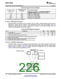
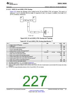
8.13.2.2.10 VREFSSTL_DDR Routing
VREFSSTL_DDR is used as a reference by the input buffers of the DDR2 memories as well as the
processor. VREF is intended to be half the DDR2 power supply voltage and should be created using a
resistive divider as shown in Figure 8-49. Other methods of creating VREF are not recommended.
Figure 8-52 shows the layout guidelines for VREF.
VREF Nominal Max Trace
width is 20 mils
DDR2 Device
VREF Bypass Capacitor
A1
A1
+
+
DDR2 Controller
Neck down to minimum in BGA escape
regions is acceptable. Narrowing to
accomodate via congestion for short
distances is also acceptable. Best
performance is obtained if the width
of VREF is maximized.
Figure 8-52. VREF Routing and Topology
226
Peripheral Information and Timings
Copyright © 2013, Texas Instruments Incorporated
Submit Documentation Feedback
Product Folder Links: DM385 DM388

 TI [ TEXAS INSTRUMENTS ]