DM385, DM388
SPRS821D –MARCH 2013–REVISED DECEMBER 2013
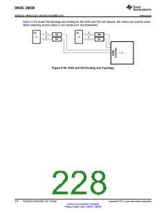
www.ti.com
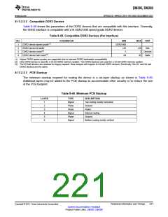
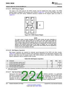
8.13.2.2.5 DDR2 Keepout Region
The region of the PCB used for the DDR2 circuitry must be isolated from other signals. The DDR2
keepout region is defined for this purpose and is shown in Figure 8-51. The size of this region varies with
the placement and DDR routing. Additional clearances required for the keepout region are shown in
Table 8-51.
A1
A1
DDR2 Device
A1
A1
Figure 8-51. DDR2 Keepout Region
NOTE
The region shown in should encompass all the DDR2 circuitry and varies depending on
placement. Non-DDR2 signals should not be routed on the DDR signal layers within the
DDR2 keepout region. Non-DDR2 signals may be routed in the region, provided they are
routed on layers separated from DDR2 signal layers by a ground layer. No breaks should be
allowed in the reference ground layers in this region. In addition, the 1.8-V power plane
should cover the entire keepout region. Routes for the DDR interface must be separated by
at least 4x; the more separation, the better.
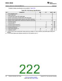
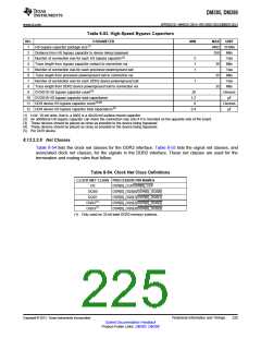
8.13.2.2.6 Bulk Bypass Capacitors
Bulk bypass capacitors are required for moderate speed bypassing of the DDR2 and other circuitry.
Table 8-52 contains the minimum numbers and capacitance required for the bulk bypass capacitors. Note
that this table only covers the bypass needs of the DDR2 interfaces and DDR2 device. Additional bulk
bypass capacitance may be needed for other circuitry.
Table 8-52. Bulk Bypass Capacitors
No. Parameter
Min
3
Max
Unit
Devices
μF
1
2
3
4
DVDD18 bulk bypass capacitor count(1)
DVDD18 bulk bypass total capacitance
DDR bulk bypass capacitor count(1)
DDR bulk bypass total capacitance(1)
30
1
Devices
μF
10
(1) These devices should be placed near the device they are bypassing, but preference should be given to the placement of the high-speed
(HS) bypass capacitors.
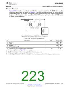
8.13.2.2.7 High-Speed Bypass Capacitors
High-speed (HS) bypass capacitors are critical for proper DDR2 interface operation. It is particularly
important to minimize the parasitic series inductance of the HS bypass capacitors, processor/DDR power,
and processor/DDR ground connections. Table 8-53 contains the specification for the HS bypass
capacitors as well as for the power connections on the PCB. Due to the number of required bypass
capacitors, it is recommended that the bypass capacitors are placed before routing the board.
224
Peripheral Information and Timings
Copyright © 2013, Texas Instruments Incorporated
Submit Documentation Feedback
Product Folder Links: DM385 DM388

 TI [ TEXAS INSTRUMENTS ]