DM385, DM388
www.ti.com
SPRS821D –MARCH 2013–REVISED DECEMBER 2013
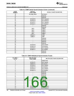
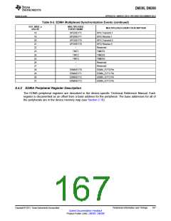
Table 8-3. EDMA Multiplexed Synchronization Events (continued)
EVT_MUX_x
VALUE
MULTIPLEXED
EVENT NAME
MULTIPLEXED EVENT DESCRIPTION
18
19
20
21
22
23
24
25
26
27
28
29
30
31
SPI2XEVT1
SPI2REVT1
SPI3XEVT0
SPI3REVT0
–
SPI2 Transmit 1
SPI2 Receive 1
SPI3 Transmit 0
SPI3 Receive 0
Reserved
TINT1
TIMER1
TINT2
TIMER2
TINT3
TIMER3
–
Reserved
–
Reserved
EDMAEVT0
EDMAEVT1
EDMAEVT2
EDMAEVT3
EDMA_EVT0 Pin
EDMA_EVT1 Pin
EDMA_EVT2 Pin
EDMA_EVT3 Pin
8.4.2 EDMA Peripheral Register Description
The EDMA peripheral registers are described in the device-specific Technical Reference Manual. Each
register is documented as an offset from a base address for the peripheral. The base addresses for all of
the peripherals are in the device memory map (see Section 2.10).
Copyright © 2013, Texas Instruments Incorporated
Peripheral Information and Timings
167
Submit Documentation Feedback
Product Folder Links: DM385 DM388

 TI [ TEXAS INSTRUMENTS ]