DM385, DM388
www.ti.com
SPRS821D –MARCH 2013–REVISED DECEMBER 2013
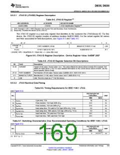
8.5.3.1 JTAG ID (JTAGID) Register Description
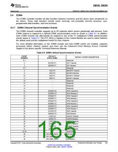
Table 8-4. JTAG ID Register(1)
HEX ADDRESS
ACRONYM
REGISTER NAME
JTAG Identification Register(2)
0x4814 0600
JTAGID
(1) IEEE Standard 1149.1-1990 Standard-Test-Access Port and Boundary Scan Architecture.
(2) Read-only. Provides the device 32-bit JTAG ID.
The JTAG ID register is a read-only register that identifies to the customer the JTAG/device ID. For this
device, the JTAG ID register resides at address location 0x4814 0600. For the actual register bit names
and their associated bit field descriptions, see Figure 8-5 and Table 8-5.
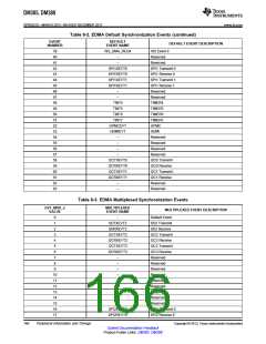
31
28 27
12 11
1
0
VARIANT (4-
PART NUMBER (16-bit)
R-1011 1001 0110 1011
MANUFACTURER (11-bit)
R-0000 0010 111
LSB
R-1
bit)
R-xxxx
LEGEND: R/W = Read/Write; R = Read only; -n = value after reset
Figure 8-5. JTAG ID Register Description - Device Register Value: 0x0B8F 202F
Table 8-5. JTAG ID Register Selection Bit Descriptions
Bit
Field
Description
31:28
VARIANT
Variant (4-bit) value. Device value: xxxx. This value reflects the device silicon revision [For example, 0x0
(0000) for initial silicon (1.0)]. For more detailed information on the current device silicon revision, see the
device-specific Silicon Errata.
27:12
11:1
0
PART NUMBER
Part Number (16-bit) value. Device value: 0xB96B (1011 1001 0110 1011)
MANUFACTURER Manufacturer (11-bit) value. Device value: 0x017 (0000 0010 111)
LSB LSB. This bit is read as a ""1 for this device.
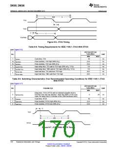
8.5.3.2 JTAG Electrical Data/Timing
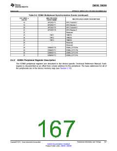
Table 8-6. Timing Requirements for IEEE 1149.1 JTAG
(see Figure 8-6)
OPP100/OPP120/
Turbo/Nitro
NO.
UNIT
MIN
59
MAX
1
tc(TCK)
1a tw(TCKH)
1b tw(TCKL)
Cycle time, TCK
ns
ns
ns
ns
ns
ns
ns
Pulse duration, TCK high (40% of tc)
23.6
23.6
5.9
Pulse duration, TCK low (40% of tc)
3
3
tsu(TDI-TCK)
Input setup time, TDI valid to TCK high (20% of (tc * 0.5))
Input setup time, TMS valid to TCK high (20% of (tc * 0.5))
Input hold time, TDI valid from TCK high
Input hold time, TMS valid from TCK high
tsu(TMS-TCK)
th(TCK-TDI)
th(TCK-TMS)
5.9
29.5
29.5
4
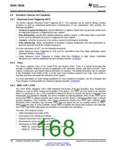
Table 8-7. Switching Characteristics Over Recommended Operating Conditions for IEEE 1149.1 JTAG
(see Figure 8-6)
OPP100/OPP120/
Turbo/Nitro
NO.
PARAMETER
UNIT
MIN
MAX
2
td(TCKL-TDOV)
Delay time, TCK low to TDO valid
0
23.575(1)
ns
(1) (0.5 * tc) - 2
Copyright © 2013, Texas Instruments Incorporated
Peripheral Information and Timings
169
Submit Documentation Feedback
Product Folder Links: DM385 DM388

 TI [ TEXAS INSTRUMENTS ]