DM385, DM388
SPRS821D –MARCH 2013–REVISED DECEMBER 2013
www.ti.com
1
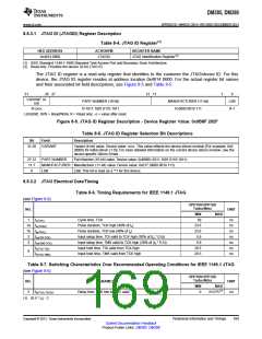
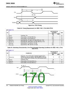
1a
1b
TCK
TDO
2
3
4
TDI/TMS
Figure 8-6. JTAG Timing
Table 8-8. Timing Requirements for IEEE 1149.1 JTAG With RTCK
(see Figure 8-6)
OPP100/OPP120/
Turbo/Nitro
NO.
UNIT
MIN
MAX
1
tc(TCK)
Cycle time, TCK
59
ns
ns
ns
ns
ns
ns
ns
1a tw(TCKH)
1b tw(TCKL)
Pulse duration, TCK high (40% of tc)
23.6
23.6
5.9
Pulse duration, TCK low (40% of tc)
3
3
tsu(TDI-TCK)
Input setup time, TDI valid to TCK high (20% of (tc * 0.5))
Input setup time, TMS valid to TCK high (20% of (tc * 0.5))
Input hold time, TDI valid from TCK high
Input hold time, TMS valid from TCK high
tsu(TMS-TCK)
th(TCK-TDI)
th(TCK-TMS)
5.9
29.5
29.5
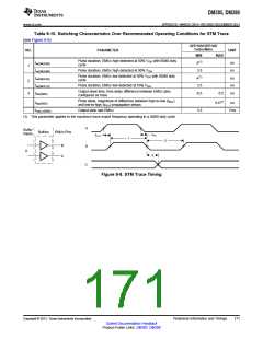
4
Table 8-9. Switching Characteristics Over Recommended Operating Conditions for IEEE 1149.1 JTAG
With RTCK
(see Figure 8-7)
OPP100/OPP120/
Turbo/Nitro
NO.
PARAMETER
UNIT
MIN
MAX
Delay time, TCK to RTCK with no selected subpaths (that is,
ICEPick is the only tap selected - when the ARM is in the scan
chain, the delay time is a function of the ARM functional clock.)
5
td(TCK-RTCK)
0
24
ns
6
7
8
tc(RTCK)
Cycle time, RTCK
59
23.6
23.6
ns
ns
ns
tw(RTCKH)
tw(RTCKL)
Pulse duration, RTCK high (40% of tc)
Pulse duration, RTCK low (40% of tc)
5
TCK
6
7
8
RTCK
Figure 8-7. JTAG With RTCK Timing
170
Peripheral Information and Timings
Copyright © 2013, Texas Instruments Incorporated
Submit Documentation Feedback
Product Folder Links: DM385 DM388

 TI [ TEXAS INSTRUMENTS ]