DLPA2000
ZHCSCO5B –JUNE 2014–REVISED FEBRUARY 2018
www.ti.com.cn
Interrupt events include fault conditions such as power-good faults, over-voltage, over-temperature shutdown,
and UVLO. For all interrupt conditions see the interrupt register on Figure 28.
The MASK register is used to mask events from generating interrupts, that is, from pulling the INTZ pin low. The
MASK settings affect the INTZ pin only and have no impact on protection and monitor circuits themselves. When
an interrupt is masked, the event causing the interrupt still sets the corresponding bit in the INT register.
However, it does not pull the INTZ pin low.
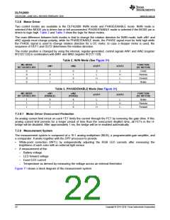
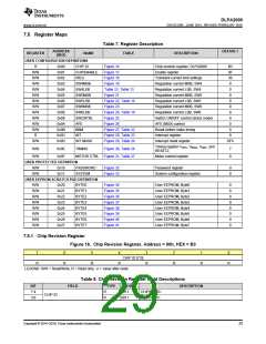
7.3.10.9 SPI
DLPA2000 provides a 4-wire SPI port that supports high-speed serial data transfers up to 33.3 MHz. Support
includes register and data buffer write and read operations. The SPI_CSZ input serves as the active low chip
select for the SPI port. The SPI_CSZ input must be forced low in order to write or read registers and data
buffers. When SPI_CSZ is forced high, the data at the SPI_DIN input is ignored, and the SPI_DOUT output is
forced to a high-impedance state. The SPI_DIN input serves as the serial data input for the port; the SPI_DOUT
output serves as the serial data output. The SPI_CLK input serves as the serial data clock for both the input and
output data. Data is latched at the SPI_DIN input on the rising edge of SPI_CLK, while data is clocked out of the
SPI_DOUT output on the falling edge of SPI_CLK. Figure 14 shows the SPI port protocol. Byte 0 is referred to as
the command byte, where the most significant bit is the write/not read bit. For the W/nR bit, a 1 indicates a write
operation, while a 0 indicates a read operation. The remaining seven bits of the command byte are the register
address targeted by the write or read operation. The SPI port supports write and read operations for multiple
sequential register addresses through the implementation of an auto-increment mode. As shown in Figure 14,
the auto-increment mode is invoked by simply holding the SPI_CSZ input low for multiple data bytes. The
register address is automatically incremented after each data byte transferred, starting with the address specified
by the command byte. After reaching address 0x7Fh the address pointer jumps back to 0x00h.
Set SPI_CSZ = 1 here to write/read one register location
Hold SPI_CSZ = 0 to enable auto-increment mode
SPI_CSZ
SPI_DIN
Header
Register Data (write)
Byte0
Byte1
Byte2
Byte3
ByteN
Register Data (read)
Data for A[6:0]
Data for A[6:0] + 1
SPI_DOUT
SPI_CLK
Data for A[6:0] + (N – 2)
Byte 0
Byte 1
W/nR
W/nR
SPI_DIN
A6 A5 A4 A3 A2 A1 A0 N7 N6 N5 N4 N3 N2 N1 N0
Set high for write, low for read
Register Address
SPI_CLK
Figure 14. SPI Protocol
7.3.11 Password Protected Registers
Register addresses 0x11h through 0x27h can be read-accessed the same way as any other register, but are
protected against accidental write operations through the PASSWORD register (address 0x10h). To write to a
protected register, follow these steps:
1. Write data 0xBAh to register address 0x10h.
2. Write data 0xBEh to register address 0x10h.
Both writes must be consecutive, that is, there must be no other read or write operation in between sending the
two bytes. After the password has been successfully written, registers 0x11h through 0x27h are unlocked and
can be write accessed using the regular SPI protocol. They remain unlocked until any byte other than 0xBAh is
written to the PASSWORD register or the part is power cycled.
To check if the registers are unlocked, read back the PASSWORD register. If the data returned is 0x00h, the
registers are locked. If the PASSWORD register returns 0x01h, the registers are unlocked.
26
Copyright © 2014–2018, Texas Instruments Incorporated

 TI [ TEXAS INSTRUMENTS ]