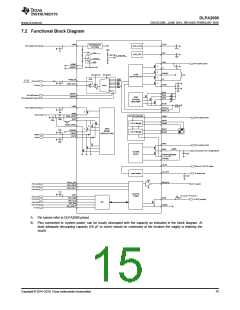
DLPA2000
www.ti.com.cn
ZHCSCO5B –JUNE 2014–REVISED FEBRUARY 2018
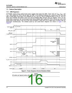
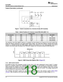
For a common-anode RGB LED configuration, the buck-boost output voltage (VLED) assumes a value such that
the voltage drop across the sense resistor equals:
(SW4_IDAC[9:0]Ivalue + ILED) × RLIM
(1)
The exact value of VLED depends on the current setting and the voltage drop across the LED but is limited to
5.4 V. When the STROBE decoder switches from SW4 to SW5, the buck-boost assumes a new output voltage
such that the sense voltage equals:
(SW5_IDAC[9:0]Ivalue + ILED) × RLIM
(SW6_IDAC[9:0]Ivalue + ILED) × RLIM
(2)
(3)
The relationship between VIN, VLED, and MAX ILED is shown in Figure 4.
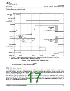
7.3.4 Calculating Inductor Peak Current
To properly configure the DLPA2000 device, a 2.2-µH inductor must be connected between pin L1 and pin L2.
The peak current for the inductor in steady state operation can be calculated.
Equation 4 shows how to calculate the peak current I1 in step down mode operation, and Equation 5 shows how
to calculate the peak current I2 in boost mode operation. VIN1 is the maximum input voltage, VIN2 is the minimum
input voltage, f is the switching frequency (2.25 MHz), and L the inductor value (2.2 µH).
VOUT
VIN1 - VOUT
IOUT
0.8
(
)
I1 =
+
2ì VIN1 ì f ìL
(4)
V
V
- V
VOUT ìIOUT
(
)
IN2
OUT IN2
I2 =
+
0.8ì V
2ì VOUT ì f ìL
IN2
(5)
The critical current value for selecting the right inductor is the higher value of I1 and I2. Also consider that load
transients and error conditions may cause higher inductor currents. This needs to be accounted for when
selecting an appropriate inductor. Internally the switching current is limited to a maximum of 4 A.
7.3.5 LED Current Accuracy
The LED drive current is controlled by a current digital-to-analog converter (DAC) and can be set independently
for switch SW4, SW5, and SW6. The DAC is trimmed at a current of 750 mA for the DLPA2000 at code: 0x307h.
The DLPA2000 current step size is 0.95 mA.
First order gain-error of the DAC can be neglected, but an offset current error must be taken into account. This
offset error differs depending on the used RLIM and will be ±25 mA for the DLPA2000 for a 100-mΩ current sense
resistor.
The max current of the DLPA2000 (SWx_IDAC[9:0] = 0x307h) is regulated to 750 mA. At the lowest setting
(SWx_IDAC[9:0] = 0x001h) the current is regulated to 14 mA for the DLPA2000. For this current setting
(0x001h), the absolute current error results into a large relative error; however, this is not a typical operating
point.
Be aware that the LED current setting not only depends on the accuracy of the RLIM resistor, but also strongly
depends on the added resistance of PCB traces and soldering quality. Due to the low value of the current sense
resistor RLIM, any extra introduced resistance (for example several mΩ) will result in a noticeable different LED
current.
Copyright © 2014–2018, Texas Instruments Incorporated
19

 TI [ TEXAS INSTRUMENTS ]