DLPA2000
ZHCSCO5B –JUNE 2014–REVISED FEBRUARY 2018
www.ti.com.cn
Feature Description (continued)
VLED
SW4
SW5
SW6
R
G
B
SW4
SW5
SW6
RLIM
RLIM_K
RLIM
RBOT_K
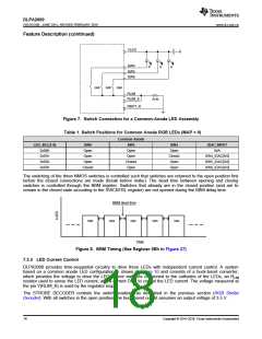
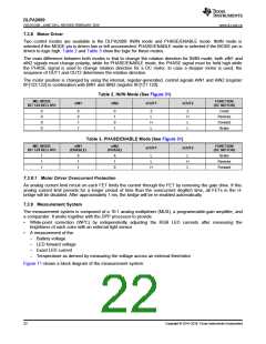
Figure 7. Switch Connection for a Common-Anode LED Assembly
Table 1. Switch Positions for Common Anode RGB LEDs (MAP = 0)
Common Anode
LED_SEL[1:0]
0x00h
SW6
Open
Open
Open
Closed
SW5
Open
Open
Closed
Open
SW4
Open
Closed
Open
Open
IDAC INPUT
N/A
0x01h
SW4_IDAC[9:0]
SW5_IDAC[9:0]
SW6_IDAC[9:0]
0x02h
0x03h
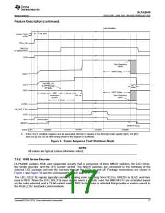
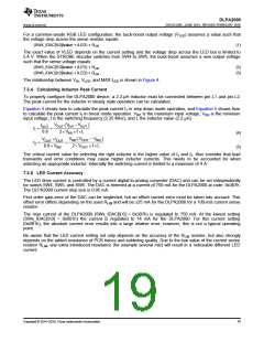
The switching of the three NMOS switches is controlled such that switches are returned to the open position first
before the closed connections are made (break before make). The dead time between opening and closing
switches is controlled through the BBM register. Switches that already are in the closed position (and are to
remain in the closed state according to the SWCNTRL register) are not opened during the BBM delay time.
BBM dead time
SW6
SW4
SW5
SW6
SW4
TIME
Figure 8. BBM Timing (See Register 0Bh in Figure 27)
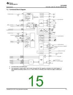
7.3.3 LED Current Control
DLPA2000 provides time-sequential circuitry to drive three LEDs with independent current control. A system
based on a common anode LED configuration is shown in Figure 10 and consists of a buck-boost converter,
which provides the voltage to drive the LEDs, three switches connected to the cathodes of the LEDs, an RLIM
resistor used to sense the LED current, and a current DAC to control the LED current. The voltage measured at
the pin V(RLIM_K) is used by the regulator loop.
The STROBE DECODER controls the switch positions as described in the previous section (RGB Strobe
Decoder). With all switches in the open position, the buck-boost output assumes an output voltage of 3.5 V.
18
Copyright © 2014–2018, Texas Instruments Incorporated

 TI [ TEXAS INSTRUMENTS ]