DLPA2000
www.ti.com.cn
ZHCSCO5B –JUNE 2014–REVISED FEBRUARY 2018
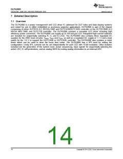
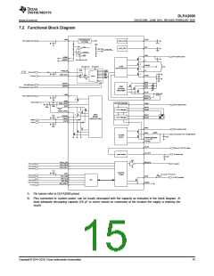
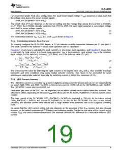
7.2 Functional Block Diagram
VINA
V2V5
REFERENCE
SYSTEM
VREF
VLED
From system power
LDO_V2V5
LDO_V6V
2.2µ
1µ
UVLO
V6V
VREF
VLED_OVP
100n
LOW_BAT
VREF
VINL
From system power
AGND
A
AGND1
SET_LOW_BAT_USB
L1
1µ
B
PGNDL
2.2µ
VLED
AFE_GAIN [1:0]
AFE_SEL[3:0]
BUCK-BOOST
C
VINA/3
VLED/3
SW4
AFE
L2
PWM_IN
From host
SW5
SW6
RLIM_K
VREF
D
CMP_OUT
VLED
22µ
To host
MUX
22µ
SW4
SENS1
From light sensor
SW5
SW6
SENS2
RGB
STROBE
DECODER
From temperature sensor
RLIM
VINR
RLIM
From system power
RLIM_K
RBOT_K
E
10µ
SWN
REF_VRST
SWP
VRST
MOTOR DRIVER
Full H-Bridge
VINM
From system power
100k
220n
Aout1
Aout2
10µ
H
CNTR_VRST
G
F
DMD
RESET
REGULATORS
Bout1
Bout2
220n
220n
PGNDR
VBIAS
VOFS
Full H-Bridge
VBIAS
VOFS
VINC
From system power
2.2uH
SWC
Vout DCDC1 (0.9-1.2V @ 450mA)
VCORE
BUCK
10µF
PGNDC/PGNDM
VCORE
LS_IN
from any 1.8V-3.3V supply
LS_OUT
to system load
Load Switch
10mF
V2V5
PROJ_ON
LED_SEL0
LED_SEL1
RESETZ
From host
From host
From host
To system
0.1u
DIGITAL
CORE
VSPI
SPI_CSZ
SPI_CLK
SPI_DIN
VIO (depends on DPP requirements)
5k
From host
From host
INTZ
To DPP (optional)
From host
From host
SPI
DGND
SPI_DOUT
To host
A. Pin names refer to DLPA2000 pinout
B. Pins connected to ‘system power’ can be locally decoupled with the capacity as indicated in the block diagram. At
least adequate decoupling capacity (50 μF or more) should be connected at the location the supply is entering the
board.
Copyright © 2014–2018, Texas Instruments Incorporated
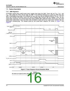
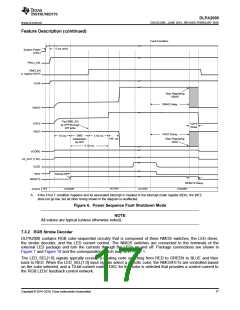
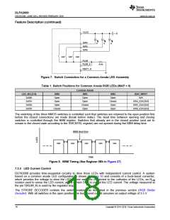
15

 TI [ TEXAS INSTRUMENTS ]