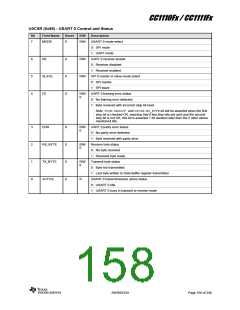
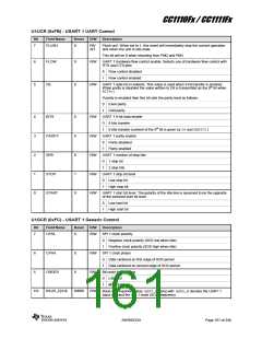
CC1110Fx / CC1111Fx
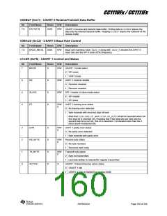
U1DBUF (0xF9) - USART 1 Receive/Transmit Data Buffer
Bit
Field Name
Reset
R/W
Description
7:0
DATA[7:0]
0x00
R/W
USART 1 receive and transmit data buffer. Writing data to U1DBUFplaces the
data into the internal transmit buffer. Reading U1DBUFreturns the contents of the
receive buffer.
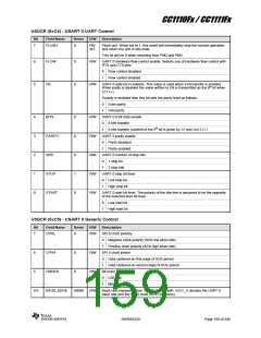
U1BAUD (0xFA) - USART 1 Baud Rate Control
Bit
Field Name
Reset
R/W
Description
7:0
BAUD_M[7:0]
0x00
R/W
Baud rate mantissa value. BAUD_Malong with BAUD_Edecides the UART 1
baud rate and the SPI 1 clock (SCK) frequency
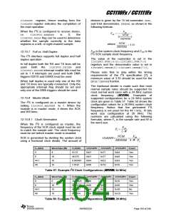
12.15 I2S
Please see Section 12.4.6.6 for details on I/O
pin mapping for the I2S interface. When the
module is in master mode, it drives the SCK
and WS lines. When the I2S interface is in slave
mode, these lines are driven by an external
master. The data on the serial data lines is
transferred one bit per SCK cycle, most
significant bit first. The WS signal selects the
channel of the current word transfer (left = 0,
right = 1). It also determines the length of each
word. There is a transition on the WS line one
bit time before the first word is transferred and
before the last bit of each word. Figure 42
shows the I2S signaling. Only a single serial
data signal is shown in this figure. The SD
signal could be the RX or TX signal depending
on the direction of the data.
The CC1110Fx/CC1111Fx provides an industry
standard I2S interface. The I2S interface can be
used to transfer digital audio samples between
the CC1110Fx/CC1111Fx and an external audio
device.
The I2S interface can be configured to operate
as master or slave and may use mono as well
as stereo samples. When mono mode is
enabled, the same audio sample will be used
for both channels. Both full and half duplex is
supported and automatic µ-Law compression
and expansion can be used.
The I2S interface consists of 4 signals:
Continuous Serial Clock (SCK)
Word Select (WS)
Serial Data In (RX)
Serial Data Out (TX)
SCK
WS
MSB
LSB
MSB
LSB
MSB
SD
SAMPLE n,
SAMPLE n+1,
SAMPLE n-1,
LEFT CHANNEL
RIGHT CHANNEL
RIGHT CHANNEL
Figure 42: I2S Digital Audio Signaling
12.15.2 I2S Interrupts
The I2S has two interrupts:
12.15.1 Enabling I2S
The I2SCFG0.ENAB bit must be set to 1 to
enable the I2S transmitter/receiver. However,
when I2SCFG0.ENAB is 0, the I2S can still be
I2S RX complete interrupt (I2SRX)
I2S TX complete interrupt (I2STX)
used
as
a
stand-alone
µ-Law
compression/expansion engine. Refer to
Section 12.15.12 on Page 165 for more details
about this.
The I2S interrupt enable bits are found in the
I2SCFG0 register. The interrupt flags are
SWRS033H
Page 162 of 246

 TI [ TEXAS INSTRUMENTS ]