CC1110Fx / CC1111Fx
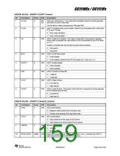
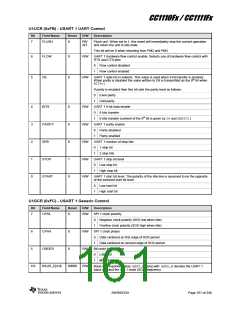
U1UCR (0xFB) - USART 1 UART Control
Bit
Field Name
Reset
R/W
Description
7
FLUSH
0
R0/
W1
Flush unit. When set to 1, this event will immediately stop the current operation
and return the unit to idle state.
This bit will be 0 when returning from PM2 and PM3
6
5
FLOW
0
0
R/W
R/W
UART 1 hardware flow control enable. Selects use of hardware flow control with
RTS and CTS pins
0
1
Flow control disabled
Flow control enabled
D9
UART 1 data bit 9 contents. This value is used when 9 bit transfer is enabled.
When parity is disabled the value written to D9 is transmitted as the 9th bit when
BIT9=1
If parity is enabled then this bit sets the parity level as follows.
0
1
Even parity
Odd parity
4
3
2
1
0
BIT9
0
0
0
1
0
R/W
R/W
R/W
R/W
R/W
UART 1 9-bit data enable
0
1
8 bits transfer
9 bits transfer (content of the 9th bit is given by D9and PARITY.)
PARITY
SPB
UART 1 parity enable
0
1
Parity disabled
Parity enabled
UART 1 number of stop bits
0
1
1 stop bit
2 stop bits
STOP
START
UART 1 stop bit level
0
1
Low stop bit
High stop bit
UART 1 start bit level. The polarity of the idle line is assumed to be the opposite
of the selected start bit level.
0
1
Low start bit
High start bit
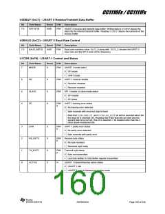
U1GCR (0xFC) - USART 1 Generic Control
Bit
Field Name
Reset
R/W
Description
7
CPOL
0
R/W
SPI 1 clock polarity
0
1
Negative clock polarity (SCK low when idle)
Positive clock polarity (SCK high when idle)
6
CPHA
0
R/W
R/W
R/W
SPI 1 clock phase
0
1
Data centered on first edge of SCK period
Data centered on second edge of SCK period
5
ORDER
0
Bit order for transfers
0
1
LSB first
MSB first
4:0
BAUD_E[4:0]
00000
Baud rate exponent value. BAUD_Ealong with BAUD_Mdecides the UART 1
baud rate and the SPI 1 clock (SCK) frequency
SWRS033H
Page 161 of 246

 TI [ TEXAS INSTRUMENTS ]