CC1110Fx / CC1111Fx
I2SDATH register, hence reading from the
I2SDATH register indicates the completion of
the read operation.
division is given by the 15 bit numerator, NUM ,
and 9-bit denominator, DENOM, as shown in the
following formula:
When the I2S is configured to receive stereo,
Fclk
NUM
Fsck
i.e.
I2SCFG0.RXMONO
is
0,
the
2(
)
I2SSTAT.RXLRflag can be used to determine
whether the sample currently in the data
registers is a left- or right-channel sample.
DENOM
NUM
DENOM
where
3.35
Fclk is the system clock frequency and Fsck is the
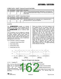
12.15.7 Full vs. Half Duplex
I2S SCK sample clock frequency.
The I2S interface supports full duplex and half
duplex operation.
The value of the numerator is set in the
I2SCLKF2.NUM[14:8]:I2SCLKF1.NUM[7:0]
In full duplex both the RX and TX lines will be
used. Both the I2SCFG0.TXIEN and
I2SCFG0.RXIENinterrupt enable bits must be
set to 1 if interrupts are used and both DMA
triggers I2STX and I2SRX must be used.
registers and the denominator value is set in
I2SCLKF2.DENOM[8]:I2SCLKF0.DENOM[7:0].
Please note that to stay within the timing
requirements of the I2S specification [7], a
minimum value of 3.35 should be used for the
(NUM/ DENOM) fraction.
When half duplex is used only one of the RX
and TX lines are typically connected. Only the
appropriate interrupt flag should be set and
only one of the DMA triggers should be used.
The fractional divider is made such that most
normal sample rates should be supported for
most normal word sizes with a 24 MHz system
clock frequency (CC1111Fx). Examples of
supported configurations for a 24 MHz system
clock are given in Table 57. Table 58 shows the
configuration values for a 26 MHz system clock
frequency. Notice that the generated I2S
frequency is not exact for the 44.1 kHz, 16 bits
word size configuration at 26 MHz. The
numbers are calculated using the following
formulas, where Fs is the sample rate and W is
the word size:
12.15.8 Master Mode
The I2S is configured as a master device by
setting I2SCFG0.MASTER to 1. When the
module is in master mode, it drives the SCK
and WS lines.
12.15.8.1 Clock Generation
When the I2S is configured as master, the
frequency of the SCK clock signal must be set
to match the sample rate. The clock frequency
must be set before master mode is enabled.
Fsck
Fs
2 W
NUM
F
clk
SCK is generated by dividing the system clock
using a fractional clock divider. The amount of
CLKDIV
DENOM 4 W Fs
I2SCLKF2 I2SCLKF1 I2SCLKF0
Fs (kHz)
Word Size (W)
CLKDIV
93.75
Exact
Yes
8
8
0x01
0x01
0x04
0x00
0x77
0x77
0xE2
0x7D
0x04
0x08
0x93
0x10
8
16
16
16
46.875
8.503401
7.8125
Yes
44.1
48
Yes
Yes
Table 57: Example I2S Clock Configurations (CC1111Fx, 24 MHz)
I2SCLKF2 I2SCLKF1 I2SCLKF0
Fs (kHz)
Word Size (W)
CLKDIV
101.5625
50.78125
9.21201
8.46354
Exact
Yes
Yes
No
8
8
0x06
0x06
0x8A
0x06
0x59
0x59
0x2F
0x59
0x10
0x20
0x1B
0xC0
8
16
16
16
44.1
48
Yes
Table 58: Example I2S Clock Configurations (CC1110Fx, 26 MHz)
SWRS033H
Page 164 of 246

 TI [ TEXAS INSTRUMENTS ]