AM3359, AM3358, AM3357
AM3356, AM3354, AM3352
www.ti.com
NO.
SPRS717F –OCTOBER 2011–REVISED APRIL 2013
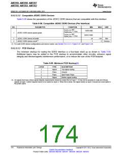
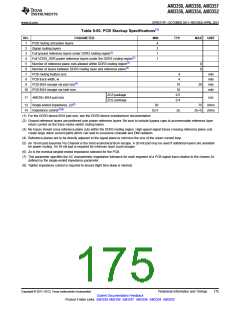
Table 5-60. PCB Stackup Specifications(1)
PARAMETER
MIN
TYP
MAX
UNIT
1
2
3
4
5
6
7
8
9
PCB routing and plane layers
4
2
1
1
Signal routing layers
Full ground reference layers under DDR3 routing region(2)
Full VDDS_DDR power reference layers under the DDR3 routing region(2)
Number of reference plane cuts allowed within DDR3 routing region(3)
Number of layers between DDR3 routing layer and reference plane(4)
PCB routing feature size
0
0
4
4
mils
mils
mils
mils
PCB trace width, w
PCB BGA escape via pad size(5)
18
10
0.5
0.4
20
10 PCB BGA escape via hole size
ZCZ package
ZCE package
11 AM335x BGA pad size
mm
13 Single-ended impedance, Zo(6)
14 Impedance control(7)(8)
50
75
ohms
ohms
Zo-5
Zo
Zo+5
(1) For the DDR3 device BGA pad size, see the DDR3 device manufacturer documentation.
(2) Ground reference layers are preferred over power reference layers. Be sure to include bypass caps to accommodate reference layer
return current as the trace routes switch routing layers.
(3) No traces should cross reference plane cuts within the DDR3 routing region. High-speed signal traces crossing reference plane cuts
create large return current paths which can lead to excessive crosstalk and EMI radiation.
(4) Reference planes are to be directly adjacent to the signal plane to minimize the size of the return current loop.
(5) An 18-mil pad assumes Via Channel is the most economical BGA escape. A 20-mil pad may be used if additional layers are available
for power routing. An 18-mil pad is required for minimum layer count escape.
(6) Zo is the nominal singled-ended impedance selected for the PCB.
(7) This parameter specifies the AC characteristic impedance tolerance for each segment of a PCB signal trace relative to the chosen Zo
defined by the single-ended impedance parameter.
(8) Tighter impedance control is required to ensure flight time skew is minimal.
Copyright © 2011–2013, Texas Instruments Incorporated
Peripheral Information and Timings
175
Submit Documentation Feedback
Product Folder Links: AM3359 AM3358 AM3357 AM3356 AM3354 AM3352

 TI [ TEXAS INSTRUMENTS ]