AM3359, AM3358, AM3357
AM3356, AM3354, AM3352
SPRS717F –OCTOBER 2011–REVISED APRIL 2013
www.ti.com
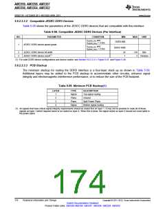
5.6.2.3.3.2 Compatible JEDEC DDR3 Devices
Table 5-58 shows the parameters of the JEDEC DDR3 devices that are compatible with this interface.
Table 5-58. Compatible JEDEC DDR3 Devices (Per Interface)
NO.
PARAMETER
CONDITION
tC(DDR_CK) and
tC(DDR_CKn) = 3.3ns
MIN
MAX
UNIT
DDR3-800
1
JEDEC DDR3 device speed grade
tC(DDR_CK) and
tC(DDR_CKn) = 2.5ns
DDR3-1600
2
3
JEDEC DDR3 device bit width
JEDEC DDR3 device count(1)
x8
1
x16
2
Bits
Devices
(1) For valid DDR3 device configurations and device counts, see Section 5.6.2.3.3.1, Figure 5-47, and Figure 5-49.
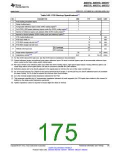
5.6.2.3.3.3 PCB Stackup
The minimum stackup for routing the DDR3 interface is a four-layer stack up as shown in Table 5-59.
Additional layers may be added to the PCB stackup to accommodate other circuitry, enhance signal
integrity and electromagnetic interference performance, or to reduce the size of the PCB footprint.
Table 5-59. Minimum PCB Stackup(1)
LAYER
TYPE
Signal
Plane
Plane
Signal
DESCRIPTION
Top signal routing
Ground
1
2
3
4
Split Power Plane
Bottom signal routing
(1) All signals that have critical signal integrity requirements should be routed first on layer 1. It may not be possible to route all of these
signals on layer 1 which requires some to be routed on layer 4. When this is done, the signal routes on layer 4 should not cross splits in
the power plane.
174
Peripheral Information and Timings
Copyright © 2011–2013, Texas Instruments Incorporated
Submit Documentation Feedback
Product Folder Links: AM3359 AM3358 AM3357 AM3356 AM3354 AM3352

 TI [ TEXAS INSTRUMENTS ]