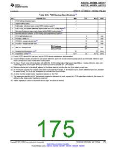
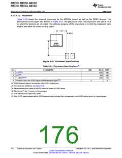
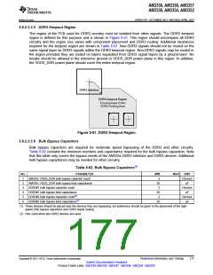
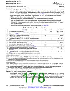
AM3359, AM3358, AM3357
AM3356, AM3354, AM3352
www.ti.com
SPRS717F –OCTOBER 2011–REVISED APRIL 2013
5.6.2.3.3.8 Net Classes
Table 5-64 lists the clock net classes for the DDR3 interface. Table 5-65 lists the signal net classes, and
associated clock net classes, for signals in the DDR3 interface. These net classes are used for the
termination and routing rules that follow.
Table 5-64. Clock Net Class Definitions
CLOCK NET CLASS AM335x PIN NAMES
CK
DDR_CK and DDR_CKn
DQS0
DQS1
DDR_DQS0 and DDR_DQSn0
DDR_DQS1 and DDR_DQSn1
Table 5-65. Signal Net Class Definitions
ASSOCIATED CLOCK
SIGNAL NET CLASS
AM335x PIN NAMES
NET CLASS
ADDR_CTRL
CK
DDR_BA[2:0], DDR_A[15:0], DDR_CSn0, DDR_CASn, DDR_RASn,
DDR_WEn, DDR_CKE, DDR_ODT
DQ0
DQ1
DQS0
DQS1
DDR_D[7:0], DDR_DQM0
DDR_D[15:8], DDR_DQM1
5.6.2.3.3.9 DDR3 Signal Termination
Signal terminations are required for the CK and ADDR_CTRL net class signals. On-device terminations
(ODTs) are required on the DQS[x] and DQ[x] net class signals. Detailed termination specifications are
covered in the routing rules in the following sections.
Figure 5-48 provides an example DDR3 schematic with a single 16-bit DDR3 memory device that does
not have VTT termination on the address and control signals. A typical DDR3 point-to-point topology may
provide acceptable signal integrity without VTT termination. System performance should be verified by
performing signal integrity analysis using specific PCB design details before implementing this topology.
5.6.2.3.3.10 DDR_VREF Routing
DDR_VREF is used as a reference by the input buffers of the DDR3 memories as well as the AM335x
device. DDR_VREF is intended to be half the DDR3 power supply voltage and is typically generated with
a voltage divider connected to the VDDS_DDR power supply. It should be routed as a nominal 20-mil wide
trace with 0.1 µF bypass capacitors near each device connection. Narrowing of DDR_VREF is allowed to
accommodate routing congestion.
5.6.2.3.3.11 VTT
Like DDR_VREF, the nominal value of the VTT supply is half the DDR3 supply voltage. Unlike
DDR_VREF, VTT is expected to source and sink current, specifically the termination current for the
ADDR_CTRL net class Thevinen terminators. VTT is needed at the end of the address bus and it should
be routed as a power sub-plane. VTT should be bypassed near the terminator resistors.
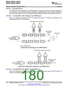
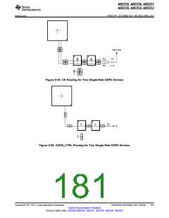
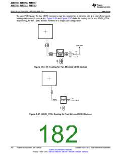
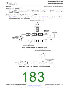
5.6.2.3.4 DDR3 CK and ADDR_CTRL Topologies and Routing Definition
The CK and ADDR_CTRL net classes are routed similarly and are length matched to minimize skew
between them. CK is a bit more complicated because it runs at a higher transition rate and is differential.
The following subsections show the topology and routing for various DDR3 configurations for CK and
ADDR_CTRL. The figures in the following subsections define the terms for the routing specification
detailed in Table 5-66.
Copyright © 2011–2013, Texas Instruments Incorporated
Peripheral Information and Timings
179
Submit Documentation Feedback
Product Folder Links: AM3359 AM3358 AM3357 AM3356 AM3354 AM3352

 TI [ TEXAS INSTRUMENTS ]