AM3359, AM3358, AM3357
AM3356, AM3354, AM3352
SPRS717F –OCTOBER 2011–REVISED APRIL 2013
www.ti.com
5.6.2.3 DDR3 and DDR3L Routing Guidelines
NOTE
All references to DDR3 in this section apply to DDR3 and DDR3L devices, unless otherwise
noted.
5.6.2.3.1 Board Designs
TI only supports board designs utilizing DDR3 memory that follow the guidelines in this document. The
switching characteristics and timing diagram for the DDR3 memory interface are shown in Table 5-56 and
Figure 5-46.
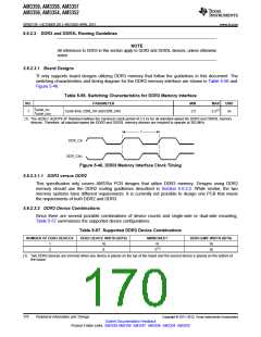
Table 5-56. Switching Characteristics for DDR3 Memory Interface
NO.
PARAMETER
MIN
MAX
UNIT
tc(DDR_CK)
tc(DDR_CKn)
1
Cycle time, DDR_CK and DDR_CKn
2.5
3.3(1)
ns
(1) The JEDEC JESD79-3F Standard defines the maximum clock period of 3.3 ns for all standard-speed bin DDR3 and DDR3L memory
devices. Therefore, all standard-speed bin DDR3 and DDR3L memory devices are required to operate at 303 MHz.
1
DDR_CK
DDR_CKn
Figure 5-46. DDR3 Memory Interface Clock Timing
5.6.2.3.1.1 DDR3 versus DDR2
This specification only covers AM335x PCB designs that utilize DDR3 memory. Designs using DDR2
memory should use the DDR2 routing guidleines described in Section 5.6.2.2. While similar, the two
memory systems have different requirements. It is currently not possible to design one PCB that meets
the requirements of both DDR2 and DDR3.
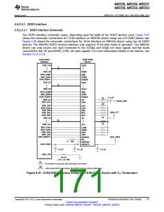
5.6.2.3.2 DDR3 Device Combinations
Since there are several possible combinations of device counts and single-side or dual-side mounting,
Table 5-57 summarizes the supported device configurations.
Table 5-57. Supported DDR3 Device Combinations
NUMBER OF DDR3 DEVICES
DDR3 DEVICE WIDTH (BITS)
MIRRORED?
DDR3 EMIF WIDTH (BITS)
1
2
16
8
N
Y(1)
16
16
(1) Two DDR3 devices are mirrored when one device is placed on the top of the board and the second device is placed on the bottom of
the board.
170
Peripheral Information and Timings
Copyright © 2011–2013, Texas Instruments Incorporated
Submit Documentation Feedback
Product Folder Links: AM3359 AM3358 AM3357 AM3356 AM3354 AM3352

 TI [ TEXAS INSTRUMENTS ]