AM3359, AM3358, AM3357
AM3356, AM3354, AM3352
SPRS717F –OCTOBER 2011–REVISED APRIL 2013
www.ti.com
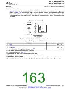
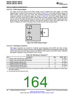
5.6.2.2.2.5 DDR2 Keepout Region
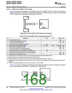
The region of the PCB used for the DDR2 circuitry must be isolated from other signals. The DDR2
keepout region is defined for this purpose and is shown in Figure 5-42. This region should encompass all
DDR2 circuitry and the region size varies with component placement and DDR2 routing. Additional
clearances required for the keepout region are shown in Table 5-47. Non-DDR2 signals should not be
routed on the same signal layer as DDR2 signals within the DDR2 keepout region. Non-DDR2 signals
may be routed in the region provided they are routed on layers separated from DDR2 signal layers by a
ground layer. No breaks should be allowed in the reference ground or VDDS_DDR power plane in this
region. In addition, the VDDS_DDR power plane should cover the entire keepout region.
A1
DDR2
Device
A1
Figure 5-42. DDR2 Keepout Region
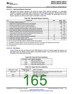
5.6.2.2.2.6 Bulk Bypass Capacitors
Bulk bypass capacitors are required for moderate speed bypassing of the DDR2 and other circuitry.
Table 5-48 contains the minimum numbers and capacitance required for the bulk bypass capacitors. Note
that this table only covers the bypass needs of the AM335x DDR2 interface and DDR2 devices. Additional
bulk bypass capacitance may be needed for other circuitry.
Table 5-48. Bulk Bypass Capacitors(1)
NO.
1
PARAMETER
AM335x VDDS_DDR bulk bypass capacitor count
AM335x VDDS_DDR bulk bypass total capacitance
DDR2#1 bulk bypass capacitor count
MIN
1
MAX
UNIT
Devices
μF
2
10
1
3
Devices
μF
4
DDR2#1 bulk bypass total capacitance
DDR2#2 bulk bypass capacitor count(2)
DDR2#2 bulk bypass total capacitance(2)
10
1
5
Devices
μF
6
10
(1) These devices should be placed near the device they are bypassing, but preference should be given to the placement of the high-speed
(HS) bypass capacitors.
(2) Only used when two DDR2 devices are used.
164
Peripheral Information and Timings
Copyright © 2011–2013, Texas Instruments Incorporated
Submit Documentation Feedback
Product Folder Links: AM3359 AM3358 AM3357 AM3356 AM3354 AM3352

 TI [ TEXAS INSTRUMENTS ]