AM3359, AM3358, AM3357
AM3356, AM3354, AM3352
www.ti.com
SPRS717F –OCTOBER 2011–REVISED APRIL 2013
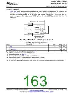
5.6.2.2.2.4 Placement
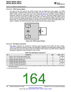
Figure 5-41 shows the required placement for the DDR2 devices. The dimensions for this figure are
defined in Table 5-47. The placement does not restrict the side of the PCB on which the devices are
mounted. The ultimate purpose of the placement is to limit the maximum trace lengths and allow for
proper routing space. For single-memory DDR2 systems, the second DDR2 device is omitted from the
placement.
X
A1
Y
OFFSET
DDR2
Y
Device
Y
OFFSET
AM335x
A1
Recommended DDR2
Device Orientation
Figure 5-41. AM335x Device and DDR2 Device Placement
Table 5-47. Placement Specifications(1)
NO.
1
PARAMETER
MIN
MAX
1750
1280
650
UNIT
mils
mils
mils
w
X(2)(3)
Y(2)(3)
Y Offset(2)(3)(4)
2
3
4
Clearance from non-DDR2 signal to DDR2 keepout region(5)(6)
4
(1) DDR2 keepout region to encompass entire DDR2 routing area.
(2) For dimension definitions, see Figure 5-41.
(3) Measurements from center of AM335x device to center of DDR2 device.
(4) For single-memory systems, it is recommended that Y offset be as small as possible.
(5) w is defined as the signal trace width.
(6) Non-DDR2 signals allowed within DDR2 keepout region provided they are separated from DDR2 routing layers by a ground plane.
Copyright © 2011–2013, Texas Instruments Incorporated
Peripheral Information and Timings
163
Submit Documentation Feedback
Product Folder Links: AM3359 AM3358 AM3357 AM3356 AM3354 AM3352

 TI [ TEXAS INSTRUMENTS ]