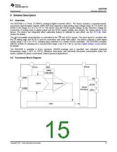
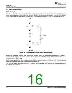
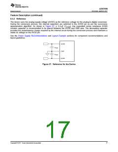
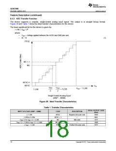
ADS7056
www.ti.com.cn
ZHCSG66 –MARCH 2017
8.4 Device Functional Modes
The device supports a simple, SPI-compatible interface to the external host. On power-up, the device is in ACQ
state. The CS signal defines one conversion and serial data transfer frame. A frame starts with a CS falling edge
and ends with a CS rising edge. The SDO pin is tri-stated when CS is high. With CS low, the clock provided on
the SCLK pin is used for conversion and data transfer and the output data are available on the SDO pin.
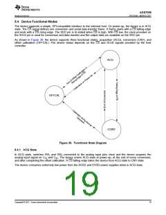
As shown in Figure 39, the device supports three functional states: acquisition (ACQ), conversion (CNV), and
offset calibration (OFFCAL). The device status depends on the CS and SCLK signals provided by the host
controller.
ACQ
OFFCAL
CONV
Figure 39. Functional State Diagram
8.4.1 ACQ State
In ACQ state, switches SW1 and SW2 connected to the analog input pins close and the device acquires the
analog input signal on CS1 and CS2. The device enters ACQ state at power-up, at the end of every conversion,
and after completing the offset calibration. A CS falling edge takes the device from ACQ state to CNV state.
The device consumes extremely low power from the AVDD and DVDD power supplies when in ACQ state.
Copyright © 2017, Texas Instruments Incorporated
19

 TI [ TEXAS INSTRUMENTS ]