ADS7056
ZHCSG66 –MARCH 2017
www.ti.com.cn
8.3 Feature Description
8.3.1 Analog Input
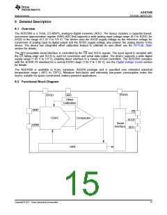
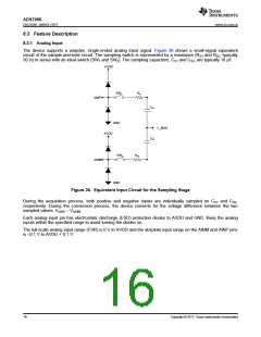
The device supports a unipolar, single-ended analog input signal. Figure 36 shows a small-signal equivalent
circuit of the sample-and-hold circuit. The sampling switch is represented by a resistance (RS1 and RS2, typically
50 Ω) in series with an ideal switch (SW1 and SW2). The sampling capacitors, CS1 and CS2, are typically 16 pF.
AVDD
SW1
Rs1
AINP
Cs1
GND
V_BIAS
AVDD
Cs2
SW2
Rs2
AINM
GND
Figure 36. Equivalent Input Circuit for the Sampling Stage
During the acquisition process, both positive and negative inputs are individually sampled on CS1 and CS2,
respectively. During the conversion process, the device converts for the voltage difference between the two
sampled values: VAINP – VAINM
.
Each analog input pin has electrostatic discharge (ESD) protection diodes to AVDD and GND. Keep the analog
inputs within the specified range to avoid turning the diodes on.
The full-scale analog input range (FSR) is 0 V to AVDD and the absolute input range on the AINM and AINP pins
is –0.1 V to AVDD + 0.1 V.
16
Copyright © 2017, Texas Instruments Incorporated

 TI [ TEXAS INSTRUMENTS ]