ADS7056
www.ti.com.cn
ZHCSG66 –MARCH 2017
9 Application and Implementation
NOTE
Information in the following applications sections is not part of the TI component
specification, and TI does not warrant its accuracy or completeness. TI’s customers are
responsible for determining suitability of components for their purposes. Customers should
validate and test their design implementation to confirm system functionality.
9.1 Application Information
The two primary circuits required to maximize the performance of a high-precision, successive approximation
register (SAR) analog-to-digital converter (ADC) are the input driver and the reference driver circuits. This section
details some general principles for designing the input driver circuit, reference driver circuit, and provides typical
application circuits designed for the device.
9.2 Typical Applications
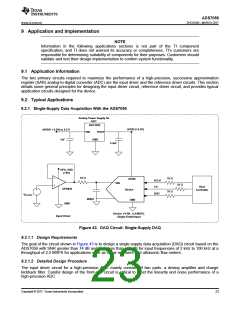
9.2.1 Single-Supply Data Acquisition With the ADS7056
Analog Power Supply for
ADC
REF1933
AVDD (+3.3V)
(AVDD + 0.2V) to 5.5 V
1uF
VIN
VOUT
GND
3.3uF
OPA_VDD
(+5V)
33 ꢀ
œ
33 ꢀ
33 ꢀ
AVDD
SCLK
CS
VIN
33 ꢀ
+
Host
OPA836
Device
+
Controller
SDO
œ
VSOURCE
680pF
GND
GND
Device: 14 Bit , 2.5 MSPS,
Single-Ended Input
Input Driver
Figure 43. DAQ Circuit: Single-Supply DAQ
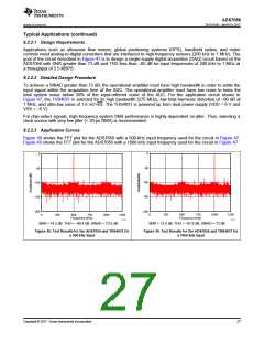
9.2.1.1 Design Requirements
The goal of the circuit shown in Figure 43 is to design a single-supply data acquisition (DAQ) circuit based on the
ADS7056 with SNR greater than 74 dB and THD less than –85 dB for input frequencies of 2 kHz to 100 kHz at a
throughput of 2.5 MSPS for applications such as sonar receivers and ultrasonic flow meters.
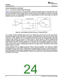
9.2.1.2 Detailed Design Procedure
The input driver circuit for a high-precision ADC mainly consists of two parts: a driving amplifier and charge
kickback filter. Careful design of the front-end circuit is critical to meet the linearity and noise performance of a
high-precision ADC.
Copyright © 2017, Texas Instruments Incorporated
23

 TI [ TEXAS INSTRUMENTS ]