ADS7056
ZHCSG66 –MARCH 2017
www.ti.com.cn
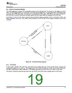
Device Functional Modes (continued)
8.4.2 CNV State
In the CNV state, the device uses the external clock to convert the sampled analog input signal to an equivalent
digital code as per the transfer function illustrated in Figure 38. The conversion process requires a minimum of
18 SCLK falling edges to be provided within the frame. After the end of conversion process, the device
automatically moves from CNV state to ACQ state. For acquisition of the next sample, a minimum time of tACQ
must be provided.
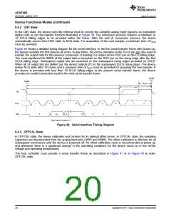
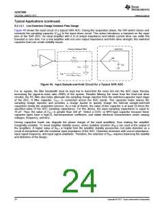
Figure 40 shows a detailed timing diagram for the serial interface. In the first serial transfer frame after power-up,
the device provides the first data as all zeros. In any frame, the clocks provided on the SCLK pin are also used to
transfer the output data for the previous conversion. A leading 0 is output on the SDO pin on the CS falling edge.
The most significant bit (MSB) of the output data is launched on the SDO pin on the rising edge after the first
SCLK falling edge. Subsequent output bits are launched on the subsequent rising edges provided on SCLK.
When all 14 output bits are shifted out, the device outputs 0's on the subsequent SCLK rising edges. The device
enters ACQ state after 18 clocks and a minimum time of tACQ must be provided for acquiring the next sample. If
the device is provided with less than 18 SCLK falling edges in the present serial transfer frame, the device
provides an invalid conversion result in the next serial transfer frame.
Sample
A+1
Sample
A
tph_CS
tCYCLE
tACQ
tCONV
CS
SCLK
SDO
1
2
3
15
16
17
18
0
D12
D0
0
0
0
D13
Data Output for Sample A-1
Figure 40. Serial Interface Timing Diagram
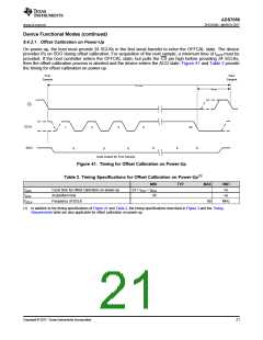
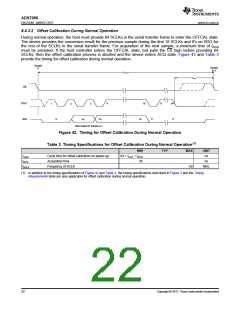
8.4.3 OFFCAL State
In OFFCAL state, the device calibrates and corrects for its internal offset errors. In OFFCAL state, the sampling
capacitors are disconnected from the analog input pins (AINP and AINM). The offset calibration is effective for all
subsequent conversions until the device is powered off. An offset calibration cycle is recommended at power-up
and whenever there is a significant change in the operating conditions for the device (such as in the AVDD
voltage and operating temperature).
The host controller must provide a serial transfer frame as described in Figure 41 or in Figure 42 to enter
OFFCAL state.
20
Copyright © 2017, Texas Instruments Incorporated

 TI [ TEXAS INSTRUMENTS ]