ADS7056
ZHCSG66 –MARCH 2017
www.ti.com.cn
Feature Description (continued)
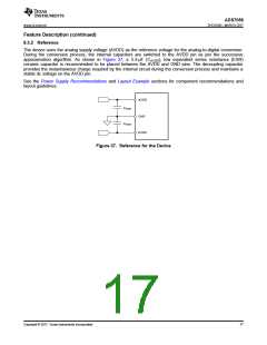
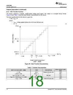
8.3.3 ADC Transfer Function
The device supports a unipolar, single-ended analog input signal. The output is in straight binary format.
Figure 38 and Table 1 show the ideal transfer characteristics for the device.
The least significant bit for the device is given by:
1 LSB = VREF / 2N
where:
•
•
VREF = Voltage applied between the AVDD and GND pins and
N = 14
(1)
PFSC
MC + 1
MC
NFSC+1
NFSC
VIN
V
REF
V
REF
VREF œ 1 LSB
+ 1LSB
1 LSB
2
2
Single-Ended Analog Input
(AINP œ AINM)
Figure 38. Ideal Transfer Characteristics
Table 1. Transfer Characteristics
IDEAL OUTPUT CODE
(Hex)
INPUT VOLTAGE (AINP – AINM)
CODE
DESCRIPTION
≤ 1 LSB
1 LSB to 2 LSBs
NFSC
NFSC + 1
MC
Negative full-scale code
0000
0001
1FFF
2000
3FFF
—
Mid code
VREF / 2 to VREF / 2 + 1 LSB
VREF / 2 + 1 LSB to VREF / 2 + 2 LSBs
≥ VREF – 1 LSB
MC + 1
PFSC
—
Positive full-scale code
18
Copyright © 2017, Texas Instruments Incorporated

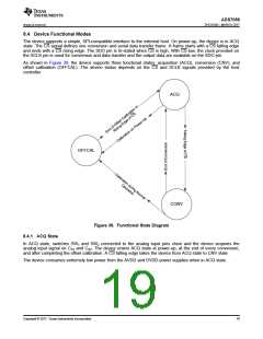
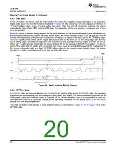
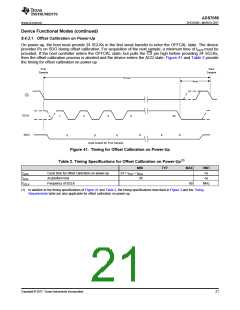
 TI [ TEXAS INSTRUMENTS ]