ADS62P49 / ADS62P29
ADS62P48 / ADS62P28
SLAS635A–APRIL 2009–REVISED JUNE 2009............................................................................................................................................................. www.ti.com
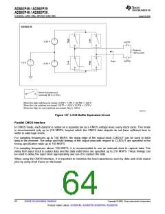
CMOS Interface Power Dissipation
With CMOS outputs, the DRVDD current scales with the sampling frequency and the load capacitance on every
output pin. The maximum DRVDD current occurs when each output bit toggles between 0 and 1 every clock
cycle. In actual applications, this condition is unlikely to occur. The actual DRVDD current would be determined
by the average number of output bits switching, which is a function of the sampling frequency and the nature of
the analog input signal.
Digital current due to CMOS output switching = CL × DRVDD × (N × FAVG),
where
CL = load capacitance,
N × FAVG = average number of output bits switching.
Figure 86 shows the current with various load capacitances across sampling frequencies at 2.5-MHz analog
input frequency
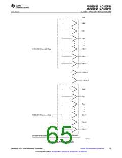
Multiplexed Output Mode (only with CMOS interface)
In this mode, the digital outputs of both the channels are multiplexed and output on a single bus (DA0-DA13
pins). The channel B output pins (DB0-DB13) are 3-stated. Since the output data rate on the DA bus is
effectively doubled, this mode is recommended only for low sampling frequencies (<65MSPS).
This mode can be enabled using register bits <POWER DOWN MODES> or using the parallel pins CTRL1-3.
Output Data Format
Two output data formats are supported – 2s complement and offset binary. They can be selected using the serial
interface register bit <DATA FORMAT> or controlling the DFS pin in parallel configuration mode.
In the event of an input voltage overdrive, the digital outputs go to the appropriate full scale level. For a positive
overdrive, the output code is 0x3FFF in offset binary output format, and 0x1FFF in 2s complement output format.
For a negative input overdrive, the output code is 0x0000 in offset binary output format and 0x2000 in 2s
complement output format.
BOARD DESIGN CONSIDERATIONS
Grounding
A single ground plane is sufficient to give good performance, provided the analog, digital, and clock sections of
the board are cleanly partitioned. See the EVM User Guide (SLAU237) for details on layout and grounding.
Supply Decoupling
As ADS62Px9/x8 already includes internal decoupling, minimal external decoupling can be used without loss in
performance. Note that decoupling capacitors can help filter external power supply noise, so the optimum
number of capacitors would depend on the actual application. The decoupling capacitors should be placed very
close to the converter supply pins.
Exposed Pad
In addition to providing a path for heat dissipation, the pad is also electrically connected to digital ground
internally. So, it is necessary to solder the exposed pad to the ground plane for best thermal and electrical
performance. For detailed information, see application notes QFN Layout Guidelines (SLOA122) and QFN/SON
PCB Attachment (SLUA271).
66
Submit Documentation Feedback
Copyright © 2009, Texas Instruments Incorporated
Product Folder Link(s): ADS62P49 / ADS62P29 ADS62P48 / ADS62P28

 TI [ TEXAS INSTRUMENTS ]