ADS62P49 / ADS62P29
ADS62P48 / ADS62P28
SLAS635A–APRIL 2009–REVISED JUNE 2009............................................................................................................................................................. www.ti.com
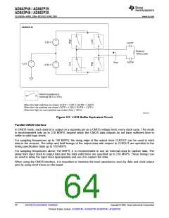
ADS62C18
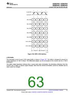
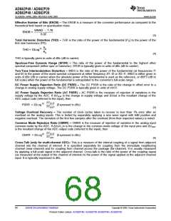
+
0.35 V
OUTP
–
External
100-W Load
+
–
OUTM
Rout
+
–
1.2 V
–0.35 V
Switch impedance is
nominally 50 W (±10%)
When the High switches are closed, OUTP = 1.375 V, OUTM = 1.025 V
When the Low switches are closed, OUTP = 1.025 V, OUTM = 1.375 V
When the High (or Low) switches are closed, Rout = 100 W
S0374-03
Figure 107. LVDS Buffer Equivalent Circuit
Parallel CMOS Interface
In CMOS mode, each data bit is output on a separate pin as a CMOS voltage level, every clock cycle. This mode
is recommended only up to 210 MSPS, beyond which the CMOS data outputs do not have sufficient time to
settle to valid logic levels.
For sampling frequencies up to 150 MSPS, the rising edge of the output clock CLKOUT can be used to latch
data in the receiver. The setup and hold timings of the output data with respect to CLKOUT are specified in the
timing specification table up to 150 MSPS.
For sampling frequencies above 150 MSPS, it is recommended to use an external clock to capture data. The
delay from input clock to output data and the data valid times are specified up to 210 MSPS. These timings can
be used to delay the input clock appropriately and use it to capture the data.
When using the CMOS interface, it is important to minimize the load capacitance seen by data and clock output
pins by using short traces on the board.
64
Submit Documentation Feedback
Copyright © 2009, Texas Instruments Incorporated
Product Folder Link(s): ADS62P49 / ADS62P29 ADS62P48 / ADS62P28

 TI [ TEXAS INSTRUMENTS ]