ADS62P49 / ADS62P29
ADS62P48 / ADS62P28
SLAS635A–APRIL 2009–REVISED JUNE 2009............................................................................................................................................................. www.ti.com
APPLICATION INFORMATION
THEORY OF OPERATION
The ADS62Px9/x8 is a family of high performance and low power dual channel 14-bit/12-bit A/D converters with
sampling rates up to 250 MSPS.
At every falling edge of the input clock, the analog input signal of each channel is sampled simultaneously. The
sampled signal in each channel is converted by a pipeline of low resolution stages. In each stage, the sampled
and held signal is converted by a high speed, low resolution flash sub-ADC. The difference (residue) between the
stage input and its quantized equivalent is gained and propagates to the next stage.
At every clock, each succeeding stage resolves the sampled input with greater accuracy. The digital outputs from
all stages are combined in a digital correction logic block and processed digitally to create the final code, after a
data latency of 22 clock cycles.
The digital output is available as either DDR LVDS or parallel CMOS and coded in either straight offset binary or
binary 2s complement format.
The dynamic offset of the first stage sub-ADC limits the maximum analog input frequency to about 500MHz (with
2V pp amplitude) and about 800MHz (with 1V pp amplitude).
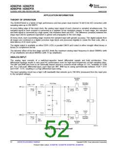
ANALOG INPUT
The analog input consists of a switched-capacitor based differential sample and hold architecture. This
differential topology results in very good AC performance even for high input frequencies at high sampling rates.
The INP and INM pins have to be externally biased around a common-mode voltage of 1.5V, available on VCM
pin. For a full-scale differential input, each input pin INP, INM has to swing symmetrically between VCM + 0.5V
and VCM – 0.5V, resulting in a 2Vpp differential input swing.
The input sampling circuit has a high 3-dB bandwidth that extends up to 700 MHz (measured from the input pins
to the sampled voltage).
Sampling
Switch
Sampling
Capacitor
RCR Filter
Lpkg » 1 nH
10 W
INP
Ron
15 W
Csamp
2 pF
Cbond
» 1 pF
Cpar2
0.5 pF
100 W
Resr
200 W
3 pF
Cpar1
0.25 pF
Ron
10 W
3 pF
100 W
Csamp
2 pF
Ron
15 W
Lpkg » 1 nH
10 W
INM
Sampling
Capacitor
Cbond
» 1 pF
Cpar2
0.5 pF
Resr
200 W
Sampling
Switch
S0322-03
Figure 93. Analog Input Circuit
52
Submit Documentation Feedback
Copyright © 2009, Texas Instruments Incorporated
Product Folder Link(s): ADS62P49 / ADS62P29 ADS62P48 / ADS62P28

 TI [ TEXAS INSTRUMENTS ]