ADS62P49 / ADS62P29
ADS62P48 / ADS62P28
www.ti.com............................................................................................................................................................. SLAS635A–APRIL 2009–REVISED JUNE 2009
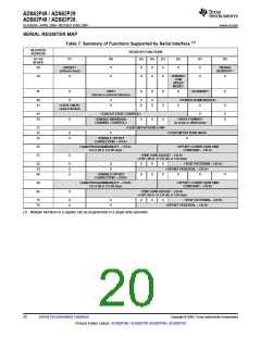
DESCRIPTION OF SERIAL REGISTERS
A7–A0 IN HEX
D7
D6
D5
D4
D3
D2
D1
D0
00
<RESET>
0
0
0
0
0
<SERIAL READOUT>
Software Reset
D7
D0
<RESET>
1 Software reset applied – resets all internal registers and self-clears to 0.
<SERIAL READOUT>
0 Serial readout disabled. SDOUT is forced low by the device (and not put in high impedance state).
1 Serial readout enabled, Pin SDOUT functions as serial data readout.
A7–A0 IN HEX
D7
D6
D5
D4
D3
D2
D1
D0
20
0
0
0
0
0
<ENABLE LOW SPEED MODE>
0
0
D2
<ENABLE LOW SPEED MODE>
0
1
LOW SPEED mode disabled. Use for sampling frequency > 100 MSPS
Enable LOW SPEED mode for sampling frequencies ≤ 100 MSPS.
A7–A0 IN HEX
D7
D6
D5
D4
D3
D2
D1
D0
3F
0
<REF>
0
0
0
<STANDBY>
0
D6-D5
<REF> Internal or external reference selection
01 Internal reference enabled
11 External reference enabled
<STANDBY>
D1
0
1
Normal operation
Both ADC channels are put in standby. Internal references, output buffers are active. This results in
quick wake-up time from standby.
A7–A0 IN HEX
D7
D6
D5
D4
D3
D2
D1
D0
40
0
0
0
0
POWER DOWN MODES
D3-D0
<POWER DOWN MODES>
0000 Pins CTRL1, CTRL2, and CTRL3 determine power down modes.
1000 Normal operation
1001 Output buffer disabled for channel B
1010 Output buffer disabled for channel A
1011 Output buffer disabled for channel A and B
1100 Global power down
1101 Channel B standby
1110 Channel A standby
1111 Multiplexed mode, MUX- (only with CMOS interface)
Channel A and B data is multiplexed and output on DA13 to DA0 pins.
Copyright © 2009, Texas Instruments Incorporated
Submit Documentation Feedback
21
Product Folder Link(s): ADS62P49 / ADS62P29 ADS62P48 / ADS62P28

 TI [ TEXAS INSTRUMENTS ]