ADS62P49 / ADS62P29
ADS62P48 / ADS62P28
www.ti.com............................................................................................................................................................. SLAS635A–APRIL 2009–REVISED JUNE 2009
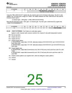
A7–A0 IN HEX
D7
D6
D5
D4
D3
D2
D1
D0
57
0
<FINE GAIN ADJUST – Common/Ch A>
+0.001 dB to +0.134 dB, in 128 steps
Using the FINE GAIN ADJUST register bits, the channel gain can be trimmed in fine steps. The trim is only
additive, has 128 steps and a range of 0.134dB. The relation between the FINE GAIN ADJUST bits and the
trimmed channel gain is:
Δ Channel gain = 20*log10[1 + (FINE GAIN ADJUST/8192)]
Note that the total device gain = ADC gain + Δ Channel gain. The ADC gain is determined by register bits
<GAIN PROGRAMMABILITY>
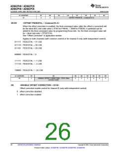
A7–A0 IN HEX
D7
D6
D5
D4
D3
D2
D1
D0
62
0
0
0
0
0
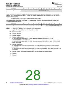
<TEST PATTERNS>
D2-D0 <TEST PATTERNS> Test Patterns to verify data capture.
Applies to both channels (with common control) or for channel A only (with independent control).
000 Normal operation
001 Outputs all zeros
010 Outputs all ones
011 Outputs toggle pattern
In ADS62P49/48, output data <D13:D0> alternates between 01010101010101 and 10101010101010
every clock cycle.
In ADS62P29/28, output data <D11:D0> alternates between 010101010101 and 101010101010 every
clock cycle.
100 Outputs digital ramp
In ADS62P49/48, output data increments by one LSB (14-bit) every clock cycle from code 0 to code
16383
In ADS62P29/28, output data increments by one LSB (12-bit) every 4th clock cycle from code 0 to
code 4095
101 Outputs custom pattern (use registers 0x51, 0x52 for setting the custom pattern)
110 Unused
111 Unused
Copyright © 2009, Texas Instruments Incorporated
Submit Documentation Feedback
25
Product Folder Link(s): ADS62P49 / ADS62P29 ADS62P48 / ADS62P28

 TI [ TEXAS INSTRUMENTS ]